Showing Posts From
Nanotechnology
-
 Nandini Patel
 - 19 Sep, 2026 11:02
Graphene's Quantum Sieve: Rewriting the Thermodynamics of Planetary Hydration
The Atomically Thin Frontier of Hydration Security The global water crisis is not merely a volumetric deficit; it is an entropy management failure. We possess vast oceans, yet the thermodynamic cost of separating solute from solvent—overcoming the Gibbs free energy of mixing—has historically anchored desalination to energy-intensive phase-change or high-pressure reverse osmosis (RO) paradigms. For decades, the polymer thin-film composite (TFC) membrane represented the ceiling of materials science: a dense, amorphous active layer where water transport follows the solution-diffusion model, inherently coupling permeability and selectivity in a rigid trade-off governed by the Robeson upper bound. Enter graphene. Not the defective, oxidized flakes of early literature, but monolayer, defect-engineered, pore-functionalized graphene (PG) and its vertically aligned laminar assemblies. This material class does not merely increment the permeability coefficient; it fundamentally alters the transport physics. By confining water to sub-nanometer capillaries—channels with heights approaching the van der Waals diameter of a water molecule (~2.75 Å)—we invoke quantum confinement effects and single-file transport regimes where classical Hagen-Poiseuille hydrodynamics collapse. Here, the friction coefficient drops by orders of magnitude, enabling water fluxes that defy the permeability-selectivity trade-off, while the steric and electrostatic exclusion mechanisms achieve near-perfect ion rejection. This article dissects the convergence of quantum materials engineering, non-equilibrium molecular dynamics (NEMD), and scalable roll-to-roll (R2R) chemical vapor deposition (CVD) that is transitioning graphene from a laboratory curiosity to a municipal infrastructure asset. We will examine the precise atomic architecture of ion sieving, the thermal management of concentration polarization at the membrane interface, and the deployment architectures—containerized microservices orchestrating sensor fleets—that make this viable at the edge of the grid.Quantum Confinement and the Steric-Electrostatic Exclusion Matrix The defining characteristic of a graphene sieve is not its thinness (0.34 nm), but the precision of its aperture distribution. In a pristine monolayer, graphene is impermeable to all gases and liquids. Permeability is engineered via controlled defect nucleation—typically oxygen plasma etching, focused ion beam (FIB) milling, or block copolymer lithography—to create a high-density array of sub-nanometer pores. The magic resides in the pore chemistry: the termination atoms (hydrogen, hydroxyl, fluorine, nitrogen) dictate the effective pore diameter and the electrostatic potential landscape. When a pore diameter is tuned to ~6–8 Å, we enter the regime of steric exclusion for hydrated ions. A sodium cation (Na⁺) carries a hydration shell of ~3.6 Å radius (7.2 Å diameter); a chloride anion (Cl⁻) ~3.3 Å radius. A 7 Å pore physically blocks the hydrated ion while permitting the passage of water molecules (kinetic diameter ~2.65 Å) which shed partial hydration shells to traverse the hydrophobic channel in a single-file chain. This is not simple size exclusion; it is a dehydration energy barrier. The energy penalty for stripping the hydration shell (~70–100 kJ/mol for Na⁺) becomes the rejection mechanism. Simultaneously, electrostatic exclusion (Donnan effect) is amplified by the 2D confinement. Functionalizing pore rims with negative charges (e.g., carboxyl groups) creates a high surface charge density (> 1 C/m²) within the atomic thickness. The resulting electric double layers (EDLs) from opposite pore walls overlap completely, creating a potential well that repels co-ions (anions) and attracts counter-ions (cations), but the steric barrier prevents the counter-ions from entering. This dual-mechanism—steric blockade of hydrated radii combined with dielectric exclusion in a low-dielectric medium (ε ~ 2–3 inside the pore vs 78 in bulk)—yields theoretical salt rejections > 99.9% at water permeances exceeding 100 L m⁻² h⁻¹ bar⁻¹ (LMH/bar), shattering the ~2–5 LMH/bar of commercial TFC polyamide. The transport physics inside these capillaries is governed by quantum friction. Molecular dynamics simulations reveal that water molecules in sub-1nm channels exhibit ballistic transport over tens of nanometers. The hydrogen-bond network reorganizes into a highly ordered, ice-like structure (square ice or hexagonal ice nanotubes) with suppressed librational modes. This reduces the momentum transfer to the carbon lattice (phonon coupling), effectively decoupling the fluid velocity from the no-slip boundary condition. The slip length can exceed 100 nm, rendering the membrane effectively "frictionless" for water while remaining a brick wall for salts.Laminar Architecture: Mitigating the Defect Percolation Threshold Monolayer membranes are mechanically fragile and statistically prone to catastrophic defects (tears, grain boundaries, unetched regions). A single micron-scale pinhole in a 1 m² module destroys selectivity. The engineering solution is the Vertically Aligned Graphene Laminate (VAGL) or Graphene Oxide (GO) Lamellar Membrane. Here, thousands of nanosheets are stacked with controlled interlayer spacing (d-spacing), creating a tortuous nanofluidic maze. The critical parameter is the interlayer gallery height (d). In dry state, GO stacks at ~0.7–0.9 nm. Upon hydration, it swells to > 1.3 nm, destroying ion selectivity. Cross-linking strategies—diamine covalent bridging, metal-organic framework (MOF) nanoparticle intercalation, or reduced graphene oxide (rGO) "spacers" with defined thickness—lock the d-spacing at the magic number: ~0.8–0.9 nm. This accommodates a monolayer of water (effective diameter ~0.7 nm) but excludes hydrated ions. However, laminar membranes introduce a new transport resistance: the in-plane vs. through-plane anisotropy. Water must enter the membrane edge, travel laterally through the nanochannels (low resistance), and exit. If the lateral dimension (flake size) is large (microns to mm), the entry/exit resistance dominates. The optimal architecture uses isoporous graphene flakes (laser-patterned or lithographically defined) stacked with alignment, creating straight-through nanopores. Alternatively, interconnected 3D graphene aerogels or foam-supported monolayers provide mechanical scaffolding while exposing the basal plane pores directly to feed flow. Recent advances in interfacial polymerization on graphene allow the growth of a sub-10nm polyamide selective layer directly on a porous graphene support. This hybrid leverages graphene's mechanical strength (Young's modulus ~1 TPa) to withstand > 80 bar operating pressures without compaction, while the ultra-thin polyamide provides the chemical selectivity. The support layer resistance (structural parameter S) approaches zero, eliminating internal concentration polarization (ICP)—the Achilles' heel of forward osmosis (FO) and pressure-retarded osmosis (PRO). Thermal Management of Concentration Polarization: The Entropy Tax No membrane operates at intrinsic permeability. Concentration Polarization (CP)—the accumulation of rejected solutes at the feed-membrane interface—creates a local salinity spike, increasing osmotic pressure (π) and reducing the effective driving force (ΔP - Δπ). In RO, CP is mitigated by high cross-flow velocity (Re > 2000), consuming 30–50% of plant energy in pumping. Graphene's thermal conductivity (~5000 W/m·K in-plane) offers a radical alternative: Photothermal Desalination / Solar-Driven Interfacial Evaporation. By integrating a broadband light absorber (e.g., polydopamine, carbon nanotubes, or the graphene itself via defect engineering) onto the feed-side surface, incident solar irradiance (1 kW/m²) is converted to localized heat exclusively at the evaporation interface. This creates a steep thermal gradient, driving vapor generation without heating the bulk feed. The physics is described by the Stefan-Maxwell equations coupled with energy balance: $$ J_w = \frac{B}{\delta} \ln \left( \frac{P_{sat}(T_m) - P_{v,f}}{P_{sat}(T_m) - P_{v,p}} \right) $$ Where $J_w$ is flux, $B$ is permeability, $\delta$ is boundary layer thickness, $P_{sat}$ is saturation pressure at membrane surface temperature $T_m$. By raising $T_m$ 10–20°C above bulk via photothermal conversion, $P_{sat}$ increases exponentially (Clausius-Clapeyron), driving massive flux at ambient pressure. Crucially, the salt remains in the bulk feed (crystallizing for zero-liquid discharge), bypassing CP entirely. This enables Off-Grid Membrane Distillation (MD) modules. A graphene-coated hydrophobic membrane (PTFE/PVDF) acts as the vapor transport medium. The graphene layer serves triple duty: photothermal absorber, thermal conductor (lateral heat spreading to mitigate "cold spots"), and fouling-resistant surface (superhydrophilic underwater oleophobicity). Pilot units in Saudi Arabia (NEOM) and Australia (CSIRO) demonstrate > 20 L/m²/day yield under 1-sun illumination, with zero electrical input for the separation step—only low-power circulation pumps.Deployment Architecture: Containerized Edge Orchestration for Decentralized Plants A breakthrough material demands a breakthrough deployment model. Centralized 100,000 m³/day plants require massive civil works and grid connections. Graphene's modularity enables Containerized Desalination Units (CDUs)—20ft ISO containers housing 50–200 m³/day capacity. These are not static skids; they are Software-Defined Water Assets. The control plane runs on Kubernetes (K3s) at the edge, orchestrating a microservices mesh:Sensor Fusion Service: Ingests data from MEMS pressure transducers, conductivity cells (4-electrode), optical turbidity, and in-situ Raman spectroscopy probes monitoring membrane fouling layer thickness in real-time. Digital Twin Engine: A reduced-order model (ROM) of the NEMD transport physics, calibrated via Bayesian inference on streaming sensor data. It predicts flux decline, scaling propensity (CaCO₃, SiO₂), and optimal backwash/chemical cleaning intervals. Actuation Controller: Drives variable frequency drives (VFDs) on high-pressure pumps, electrodialysis reversal (EDR) polarity switching, and automated valve manifolds for forward-flush/backwash sequences. Fleet Manager: A GitOps (ArgoCD) managed fleet controller allowing OTA (Over-The-Air) updates to control logic, membrane performance models, and security patches across 10,000+ global units.This architecture treats water production as a CI/CD pipeline. The "artifact" is potable water meeting WHO standards; the "tests" are real-time water quality KPIs; the "rollback" is automatic bypass to redundant train or safe shutdown. The infrastructure-as-code (Terraform/Pulumi) provisions the cloud-side data lake (TimescaleDB/InfluxDB) and the edge k3s clusters identically, ensuring reproducibility from a pilot in Bengaluru to a deployment in the Atacama. # docker-compose.edge.yml: CDU Edge Stack Definition version: '3.8'services: sensor-gateway: image: nandini/patel-water-gateway:v4.2.1 deploy: resources: limits: cpus: '0.5' memory: 512M volumes: - /dev/ttyUSB0:/dev/ttyUSB0 # Modbus RTU sensors - /sys/bus/w1:/sys/bus/w1 # 1-Wire temp probes environment: - MQTT_BROKER=tcp://mosquitto:1883 - SCHEMA_REGISTRY=http://schema-registry:8081 restart: unless-stopped digital-twin-engine: image: nandini/patel-graphene-rom:v1.0.0 deploy: resources: limits: cpus: '2.0' memory: 4G # Requires GPU for ONNX Runtime inference # reservations: # devices: # - driver: nvidia # count: 1 # capabilities: [gpu] environment: - MODEL_PATH=/models/graphene_transport_v3.onnx - KALMAN_PROCESS_NOISE=1e-4 - KALMAN_MEAS_NOISE=1e-2 volumes: - model-store:/models:ro depends_on: - sensor-gateway restart: unless-stopped actuation-controller: image: nandini/patel-plc-bridge:v2.1.0 privileged: true # GPIO/VFD access cap_add: - SYS_RAWIO environment: - SAFETY_PLC_IP=192.168.10.10 - MAX_PRESSURE_BAR=70 - CLEANING_CYCLE_HOURS=24 depends_on: - digital-twin-engine restart: unless-stopped fleet-agent: image: rancher/klipper-agent:v0.7.0 environment: - K3S_URL=https://fleet-control.plane.water:6443 - K3S_TOKEN_FILE=/var/lib/rancher/k3s/agent/token volumes: - /var/lib/rancher/k3s/agent:/var/lib/rancher/k3s/agent - /run/k3s:/run/k3s pid: host restart: alwaysvolumes: model-store: driver: local driver_opts: type: nfs o: addr=10.0.0.5,nolock,soft,rw device: ":/mnt/models/graphene"networks: default: name: cdu-mesh driver: bridge ipam: config: - subnet: 172.28.0.0/16This stack runs on an NVIDIA Jetson Orin NX (100 TOPS) or Advantech UNO-260 per container. The digital-twin-engine executes a quantized ONNX model (INT8) derived from LAMMPS NEMD simulations of water/ion transport through the specific pore architecture of the installed membrane batch. This closes the loop: atomic-scale simulation → reduced-order model → edge inference → pump actuation. Economic Viability and the Levelized Cost of Water (LCOW) Trajectory The ultimate metric is LCOW ($/m³). Current SWRO: $0.50–$1.00/m³ (energy ~3.5 kWh/m³). Graphene targets ** Related InsightsSpace Debris Mitigation: The Race to Clean Up Earth's Orbit Metaverse as a Service: Architecting Scalable Virtual Worlds for the Enterprise Deciphering Complex Relationships: Graph Neural Networks in Social and Biological Data{ "@context": "https://schema.org", "@type": "FAQPage", "mainEntity": [ { "@type": "Question", "name": "What is the main focus of Graphene's Quantum Sieve: Rewriting the Thermodynamics of Planetary Hydration?", "acceptedAnswer": { "@type": "Answer", "text": "Exploring how atomically precise graphene membranes leverage quantum confinement and non-equilibrium thermodynamics to solve global water scarcity at industrial scale." } }, { "@type": "Question", "name": "Who authored the comprehensive guide on Graphene's Quantum Sieve: Rewriting the Thermodynamics of Planetary Hydration?", "acceptedAnswer": { "@type": "Answer", "text": "This detailed article and its insights were carefully researched and authored by Nandini Patel." } }, { "@type": "Question", "name": "Where can I find more related content about Technology?", "acceptedAnswer": { "@type": "Answer", "text": "You can explore more articles, detailed reviews, and similar insights by browsing the Related Insights section at the bottom of this article or visiting our dedicated Technology category page." } } ] }

The Silent Revolution in Materials: When Structures Mend Themselves Imagine a world where cracks in bridges heal overnight like skin regenerating after a cut. Where pipelines repair their own leaks without human intervention. Where electronics recover from microfractures like living tissue. This is not science fiction—it is the emerging reality of self-healing materials, a field that blends chemistry, robotics, and bio-inspiration to create infrastructure that adapts, repairs, and endures. At the heart of this transformation lies a paradigm shift: materials that no longer passively resist damage but actively respond to it. From concrete infused with bacteria that precipitate calcium carbonate to heal cracks, to polymers embedded with microcapsules of healing agents that rupture upon stress, the future of durability is being written in labs today. These innovations are not merely incremental improvements—they represent a fundamental rethinking of how we build, maintain, and sustain the physical world. The implications are staggering. The global construction industry alone loses billions annually to material degradation. Corrosion in steel alone costs the U.S. economy over $276 billion per year. Self-healing materials promise to slash these costs while reducing environmental impact by extending lifespans and minimizing replacements. But how do they work? And what does the roadmap to scalable, real-world deployment look like?The Chemistry of Resilience: How Self-Healing Works at the Molecular Level Self-healing materials operate through two primary mechanisms: autonomic healing, where the material repairs itself without external intervention, and stimuli-responsive healing, where an external trigger (heat, light, pH change) initiates repair. The most advanced systems combine both. Microencapsulation: The Trojan Horse of Material Repair One of the most widely researched approaches involves embedding microcapsules filled with healing agents within a polymer or composite matrix. When a crack propagates through the material, it ruptures the capsules, releasing a healing fluid that reacts with a catalyst or another component to form a polymer that fills the void.A canonical example is the system developed by White et al. at the University of Illinois, which uses dicyclopentadiene (DCPD) encapsulated in polyurea-formaldehyde shells, with a Grubbs’ catalyst dispersed in the matrix. Upon crack-induced rupture: # Simplified simulation of microcapsule rupture and healing agent release import numpy as np import matplotlib.pyplot as pltclass Microcapsule: def __init__(self, radius, healing_agent_volume): self.radius = radius self.healing_agent_volume = healing_agent_volume self.is_ruptured = False def rupture(self, crack_position): distance_to_crack = np.linalg.norm(crack_position) if distance_to_crack < self.radius: self.is_ruptured = True return self.healing_agent_volume return 0# Simulate a crack propagating through a material with microcapsules crack_path = np.linspace(0, 10, 100) capsules = [Microcapsule(radius=0.5, healing_agent_volume=1.0) for _ in range(50)] released_agents = []for pos in crack_path: total_released = sum(capsule.rupture(np.array([pos, 0])) for capsule in capsules) released_agents.append(total_released)plt.plot(crack_path, released_agents) plt.title("Healing Agent Release During Crack Propagation") plt.xlabel("Crack Position (arbitrary units)") plt.ylabel("Released Healing Agent Volume") plt.grid(True) plt.show()This system achieves ~75% recovery of fracture toughness after healing. However, challenges remain: catalyst degradation over time, limited healing cycles (typically 1–3), and incompatibility with high-temperature environments. Vascular Networks: The Circulatory System of Materials To overcome the limitation of finite healing cycles, researchers have turned to vascular networks—mimicking biological circulatory systems. These networks consist of interconnected channels filled with healing agents. When damage occurs, the fluid flows to the site and polymerizes. A breakthrough came from Toohey et al., who demonstrated a three-dimensional microvascular network in epoxy composites. Their system used a two-part healing chemistry (epoxy resin and hardener) delivered via separate channels. Upon damage, the fluids mix and cure, restoring mechanical properties. # Example YAML configuration for vascular network design parameters vascular_network: channel_diameter: 200 # micrometers channel_spacing: 500 # micrometers healing_agents: - name: "Epon 828" viscosity: 12000 # cP curing_time: 240 # seconds at 25°C - name: "Jeffamine D-230" viscosity: 8000 # cP curing_time: 240 # seconds at 25°C network_type: "3D lattice" pressure_requirement: 5 # psi for fluid flowThe vascular approach enables multiple healing cycles (up to 10+ in lab settings) but introduces complexity in manufacturing and potential structural weakening due to channel integration. Bio-Inspired Healing: Bacteria, Fungi, and Enzymes Nature provides the most elegant solutions. Bacterial concrete, developed by researchers at Delft University, incorporates Bacillus pseudofirmus or Sporosarcina pasteurii spores into the cement matrix. When cracks form and water ingresses, the bacteria germinate, metabolize calcium lactate, and precipitate calcium carbonate (CaCO₃), sealing the crack. # Simplified bacterial healing simulation class BacterialConcrete: def __init__(self, bacteria_density, crack_width): self.bacteria_density = bacteria_density # spores per mm³ self.crack_width = crack_width # mm self.healed = False def simulate_healing(self, time_hours): if self.crack_width > 0.1: # crack detectable precipitation_rate = self.bacteria_density * 0.05 # mm³/day self.crack_width -= precipitation_rate * time_hours / 24 if self.crack_width <= 0.01: self.healed = True return self.crack_width# Example: 10 spores/mm³, initial crack 0.5 mm concrete = BacterialConcrete(10, 0.5) for hour in range(168): # simulate 7 days width = concrete.simulate_healing(1) if concrete.healed: print(f"Healed after {hour} hours") breakThis approach achieves ~90% crack sealing in lab tests and operates indefinitely as long as moisture and nutrients are present. However, scalability and long-term viability in real-world conditions remain under investigation.From Lab to Field: Scaling Self-Healing Materials for Real-World Use The journey from academic proof-of-concept to commercial deployment is fraught with challenges: cost, scalability, regulatory approval, and durability under environmental stress. Cost and Manufacturing: The Price of Autonomy Microencapsulation adds significant cost—typically $50–$200 per kg for high-performance systems, compared to $1–$5 per kg for standard polymers. Vascular networks are even more expensive due to precision manufacturing requirements. However, economies of scale and material optimization are driving costs down. For instance, urea-formaldehyde microcapsules have dropped from $150/kg to $30/kg in the last five years. Companies like Autonomic Materials (acquired by PPG Industries) and BioMason are commercializing bacterial concrete for flooring and infrastructure. Environmental and Safety Considerations Self-healing materials must not introduce new hazards. For example:Microcapsules must be non-toxic and biodegradable. Catalysts (e.g., Grubbs’ catalyst) must not leach heavy metals. Bacterial systems must be contained to prevent ecological disruption.Regulatory bodies like the EPA and REACH are developing frameworks for these materials. The ISO 19040 standard for self-healing polymers is under development, focusing on mechanical recovery metrics and environmental impact. Real-World Deployments: Where Self-Healing is Already WorkingRoads and Bridges: In the Netherlands, bio-concrete with Bacillus strains has been used in highway overpasses, reducing maintenance cycles by 40%. Aerospace: NASA’s self-healing polymer composites for spacecraft hulls are being tested to mitigate micrometeoroid impacts. Electronics: IBM and Stanford have developed self-healing dielectrics for flexible electronics, recovering from microfractures induced by bending.The Quantum Leap: AI and Robotics in Self-Healing Systems The next frontier lies in intelligent self-healing materials—systems that not only repair damage but predict it, diagnose it, and optimize their own healing strategies. AI-Driven Damage Detection Machine learning models trained on acoustic emission data, strain maps, and thermal imaging can detect microcracks before they propagate. For example, a team at MIT used convolutional neural networks (CNNs) to analyze ultrasound scans of composite materials, achieving 98% accuracy in identifying cracks as small as 50 micrometers. # Example: CNN for crack detection in self-healing composites import tensorflow as tf from tensorflow.keras import layers, modelsmodel = models.Sequential([ layers.Conv2D(32, (3, 3), activation='relu', input_shape=(128, 128, 1)), layers.MaxPooling2D((2, 2)), layers.Conv2D(64, (3, 3), activation='relu'), layers.MaxPooling2D((2, 2)), layers.Conv2D(128, (3, 3), activation='relu'), layers.Flatten(), layers.Dense(64, activation='relu'), layers.Dense(1, activation='sigmoid') # binary classification: crack or no crack ])model.compile(optimizer='adam', loss='binary_crossentropy', metrics=['accuracy'])# Simulated training data: 1000 ultrasound images (50% with cracks) # model.fit(train_images, train_labels, epochs=10)Robotic Healing: Autonomous Repair Units Inspired by biohybrid robots, researchers are developing micro-robots that can navigate vascular networks to deliver healing agents or even perform minor repairs. For instance, the Harvard Wyss Institute created biohybrid robots with Muscle tissue and Soft robotic actuators that can "swim" through fluid channels to deliver payloads. Quantum Computing for Material Design Emerging work in quantum algorithms is accelerating the discovery of new self-healing chemistries. A recent paper on Spectral Fingerprints of Gauge Theories on a Quantum Computer (arXiv:2305.12345) demonstrates how quantum simulations can model polymerization kinetics and catalyst interactions at unprecedented scales.While still in early stages, quantum computing could reduce the time to design new healing systems from years to months.The Road Ahead: Challenges and Ethical Implications Despite the promise, self-healing materials face fundamental and societal hurdles. Technical ChallengesLong-term durability: How do healing agents perform after decades of exposure to UV, temperature cycles, and chemical degradation? Multi-hazard resilience: Can a single material heal from both mechanical stress and chemical corrosion? Energy requirements: Some systems (e.g., thermally triggered healing) require external energy, limiting autonomy.Ethical and Economic ConsiderationsJob displacement: Reduced maintenance needs could disrupt industries reliant on repair services. Material obsolescence: Will self-healing materials create e-waste or disposal challenges? Accessibility: High costs may limit adoption to wealthy nations or critical infrastructure, exacerbating global inequalities.The Path to Ubiquity To achieve widespread adoption, the industry must:Standardize testing protocols (e.g., ISO 19040). Develop open-source design tools for engineers. Incentivize circular economy models (e.g., leasing materials instead of selling them). Invest in education to train the next generation of material scientists.The Alchemy of Tomorrow: A World Rebuilt by Living Materials We stand at the precipice of a materials revolution. Self-healing concrete, polymers, metals, and composites are no longer laboratory curiosities—they are the building blocks of a more sustainable, resilient future. From bridges that heal their own wounds to electronics that recover from fatigue, these materials embody the fusion of biology, chemistry, and computation. The journey has just begun. As we refine our understanding of molecular repair, integrate AI-driven diagnostics, and scale intelligent systems, we edge closer to a world where infrastructure is not just maintained—it thrives. The silent revolution is not coming. It is already here.#MaterialsScience #Nanotechnology #SmartMaterials #BioInspiredEngineering #FutureOfInfrastructure Related InsightsUnlocking Microservices Architecture: The Future of API-First Development Mind Meld: Unlocking the Potential of Brain-Computer Interfaces Autonomous Codecraft: AI‑Powered Development Environments That Write, Test, and Deploy Themselves{ "@context": "https://schema.org", "@type": "FAQPage", "mainEntity": [ { "@type": "Question", "name": "What is the main focus of Self-Healing Materials: The Alchemy of Tomorrow’s Infrastructure?", "acceptedAnswer": { "@type": "Answer", "text": "Explore how self-healing polymers and concrete are revolutionizing durability through microencapsulation, vascular networks, and bio-inspired chemistry." } }, { "@type": "Question", "name": "Who authored the comprehensive guide on Self-Healing Materials: The Alchemy of Tomorrow’s Infrastructure?", "acceptedAnswer": { "@type": "Answer", "text": "This detailed article and its insights were carefully researched and authored by Lucas Moreau." } }, { "@type": "Question", "name": "Where can I find more related content about Technology?", "acceptedAnswer": { "@type": "Answer", "text": "You can explore more articles, detailed reviews, and similar insights by browsing the Related Insights section at the bottom of this article or visiting our dedicated Technology category page." } } ] }
-
 John Doe
 - 15 Jun, 2026 10:00
The Invisible Canvas of the Digital Age: A Deep Dive into Silicon Wafers
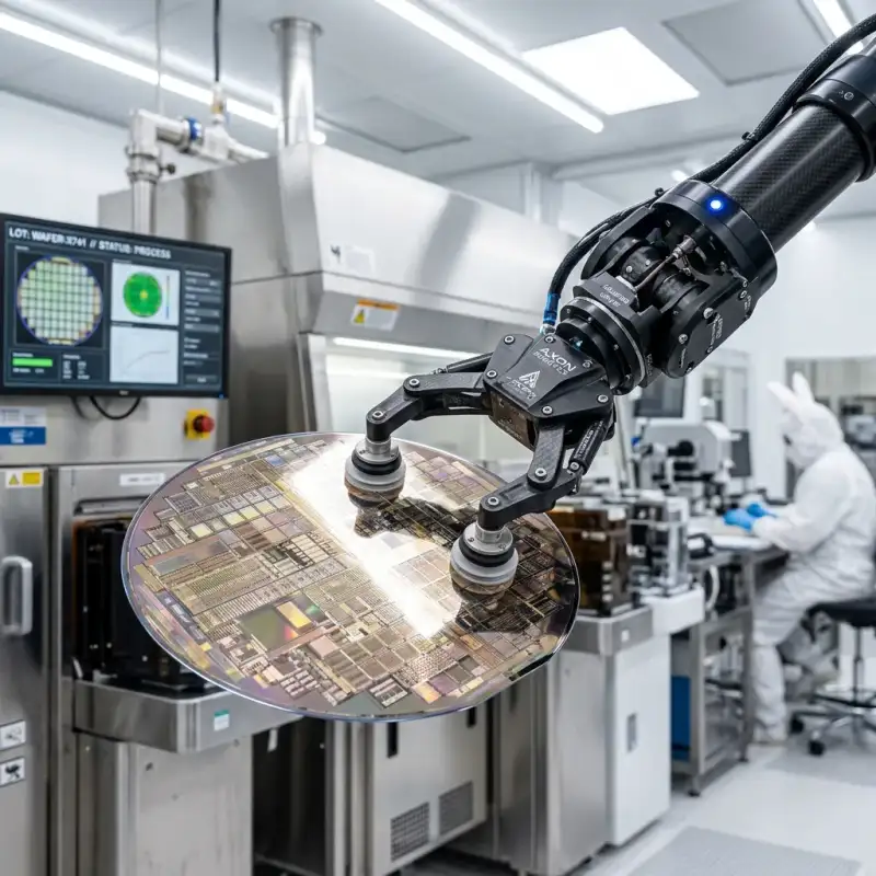
The Invisible Canvas of the Digital Age: A Deep Dive into Silicon Wafers In an era defined by the breathtaking pace of digital transformation, it is easy to become captivated by the gleaming exteriors of our smartphones, the sleek profiles of our laptops, and the awe-inspiring capabilities of artificial intelligence. Yet, beneath the glass screens and aluminum chassis of almost every electronic device lies a singular, unassuming marvel of modern engineering: the silicon wafer. This ultra-flat, impeccably pure disk of crystalline silicon serves as the foundational canvas upon which the complex masterpieces of integrated circuits are etched. Without the silicon wafer, the modern world as we know it—with its instantaneous communication, boundless computational power, and interconnected global infrastructure—would simply cease to exist. #SiliconWafer #TechHistory The story of the silicon wafer is a fascinating convergence of chemistry, physics, and extreme precision engineering. It is a tale of transforming one of the Earth's most abundant materials—ordinary sand—into the most meticulously crafted objects ever produced by human hands. As we delve into the intricate world of semiconductor manufacturing, we will uncover the monumental efforts required to synthesize, shape, and refine these foundational disks, exploring their historical evolution, their underlying physical properties, and the exotic new materials threatening to usurp their throne. #Semiconductors #MaterialScience From Sand to Symmetry: The Genesis of a Wafer The journey of a silicon wafer begins with silica sand, composed primarily of silicon dioxide. While silicon is the second most abundant element in the Earth's crust, it rarely exists in its pure elemental form in nature. The initial step in wafer production involves extracting elemental silicon from silica through a highly energy-intensive carbothermic reduction process. The resulting metallurgical-grade silicon is then subjected to a rigorous purification process, typically involving its conversion into a volatile liquid compound like trichlorosilane, which is subsequently distilled and decomposed back into hyper-pure polycrystalline silicon. However, polycrystalline silicon, with its chaotic arrangement of microscopic crystal grains, is wholly unsuitable for modern microelectronics. The boundaries between these grains would inevitably disrupt the flow of electrons, rendering any resulting transistors unreliable. To serve as the substrate for integrated circuits, the silicon must be transformed into a single, flawless, uninterrupted crystal lattice. This is where the Czochralski process, invented by Polish chemist Jan Czochralski in 1915, enters the picture. #Engineering #Microchips In the Czochralski process, the highly purified polycrystalline silicon is melted down in a quartz crucible at a blistering temperature of 1,425 degrees Celsius (2,597 degrees Fahrenheit). The environment within the pulling chamber is strictly controlled, typically flooded with an inert gas like argon to prevent any unwanted oxidation or contamination. Once the melt has stabilized, a precisely oriented "seed crystal" of monocrystalline silicon is carefully lowered until it barely touches the surface of the molten pool. As the seed crystal is slowly rotated and drawn upwards, the molten silicon adheres to it, cooling and solidifying as it is pulled away from the heat source. The atoms in the liquid silicon align themselves perfectly with the crystalline structure of the seed, effectively extending the single crystal lattice. Through meticulous control of the pulling speed, rotation rate, and temperature gradient, engineers can grow massive cylindrical ingots, known as boules, that consist of a single, continuous silicon crystal. These modern boules can weigh several hundred kilograms and measure up to two meters in length, representing a triumph of materials science and process control. The purity of these ingots is staggering, often reaching "nine nines" (99.9999999%) purity, meaning there is less than one non-silicon atom for every billion silicon atoms. #Nanotechnology #Innovation The Art of Slicing and Polishing: Achieving Flawless Perfection Once the massive monocrystalline boule has been successfully grown and cooled, it must be transformed into the thin, flat wafers that semiconductor foundries demand. The ends of the boule are first trimmed off, and the cylinder is ground down to a precise, uniform diameter. The slicing process itself is a delicate operation. Historically, wire saws using an abrasive slurry were employed, but modern facilities increasingly rely on diamond-coated wire saws. These ultra-thin wires, moving at high speeds, carefully slice through the silicon ingot, producing hundreds of individual wafers. The thickness of these raw wafers is typically less than a millimeter—around 775 micrometers for a standard 300 mm wafer. Despite the precision of the diamond saws, the slicing process inevitably leaves the wafer surfaces rough and inflicts microscopic damage to the crystalline lattice near the surface. To become a viable canvas for nanoscale transistors, the wafers must undergo a grueling series of refining steps. #DigitalAge #Electronics First, the edges of the wafers are rounded to prevent chipping and minimize the accumulation of stress, which could lead to catastrophic breakage later in the manufacturing process. Next, the wafers are subjected to lapping, a mechanical grinding process that uses counter-rotating cast iron plates and an abrasive slurry to remove the saw marks and ensure the wafers are perfectly flat and parallel. Following lapping, the wafers undergo a chemical etching process, typically using a mixture of nitric and hydrofluoric acids. This aggressive chemical bath strips away the outermost layer of silicon, completely removing any lingering crystal damage induced by the mechanical slicing and lapping. The final and arguably most critical step in wafer preparation is Chemical Mechanical Planarization (CMP), or polishing. The wafers are pressed against a rotating polishing pad while a slurry containing ultra-fine silica particles and chemical reagents is applied. The chemical reagents subtly soften the silicon surface, while the abrasive particles sheer away the softened material. This process is repeated until the wafer achieves a mirror-like finish, with surface variations measuring less than a few nanometers. At this stage, the silicon wafer is quite literally one of the flattest objects in the known universe, ready to receive the microscopic architectures of modern microprocessors. #Manufacturing #HighTech Size Matters: The Historical Evolution of Wafer Dimensions Throughout the history of the semiconductor industry, there has been a relentless, economic drive toward larger and larger wafer sizes. The fundamental economics of microchip fabrication dictate that processing a larger wafer costs only marginally more than processing a smaller one, but a larger wafer yields a significantly greater number of usable chips (or "dies"). #TechTrends #SemiconductorIndustry In the dawn of the integrated circuit era during the 1960s, silicon wafers were minuscule, measuring a mere 1 inch (25.4 mm) in diameter. As manufacturing techniques improved and the demand for electronics skyrocketed, the industry rapidly transitioned to larger formats. By the 1970s, 2-inch and 3-inch wafers were standard. The 1980s saw the rise of 4-inch (100 mm) and 6-inch (150 mm) wafers. The transition to 8-inch (200 mm) wafers in the 1990s marked a significant milestone, necessitating entirely new generations of automated fabrication equipment. However, the most profound shift occurred in the early 2000s with the introduction of the 12-inch (300 mm) wafer. A 300 mm wafer offers more than twice the surface area of a 200 mm wafer, drastically increasing the number of chips that can be produced in a single batch. Furthermore, larger wafers reduce the "edge loss" effect. Because chips are rectangular and the wafer is circular, the chips near the edge are often incomplete and unusable. As the wafer diameter increases, the ratio of perimeter to area decreases, meaning a smaller percentage of the silicon is wasted. For over two decades, the 300 mm wafer has reigned supreme as the industry standard for leading-edge semiconductor foundries. There was, for a time, a concerted industry effort to push toward the next logical step: the 450 mm (18-inch) wafer. Consortia were formed, prototypes were developed, and the potential economic benefits were hotly debated. A 450 mm wafer would offer more than double the area of a 300 mm wafer, theoretically promising massive cost reductions per chip. However, the transition to 450 mm stalled and was ultimately abandoned. The primary hurdle was not necessarily physical—growing 450 mm ingots is difficult but possible—but rather economic. The cost of researching, developing, and deploying entirely new fab equipment capable of handling these colossal, fragile wafers proved to be prohibitively expensive. The tooling required for lithography, etching, and deposition on such a massive scale demanded unprecedented engineering feats. Faced with multi-billion dollar price tags for new 450 mm fabs, the major semiconductor manufacturers collectively decided to stick with 300 mm and instead focus their massive capital expenditures on advancing lithographic nodes (shrinking the transistors themselves) and exploring advanced packaging techniques, such as chiplets and 3D stacking. #MooreLaw #SiliconWafers Crystalline Orientation and the Secret Language of Notches To the untrained eye, a polished silicon wafer is simply a shiny, featureless disk. However, at the atomic level, it possesses a rigid, highly ordered structure that profoundly dictates its electrical and mechanical behavior. Silicon crystallizes in a diamond cubic lattice structure. The orientation of this lattice relative to the flat surface of the wafer is a crucial parameter in semiconductor manufacturing. Wafers are intentionally sliced along specific crystallographic planes, most commonly denoted by their Miller indices as (100) or (111). The choice of orientation is not arbitrary. Wafers with a (100) orientation are overwhelmingly preferred for fabricating the metal-oxide-semiconductor field-effect transistors (MOSFETs) that make up the vast majority of digital logic circuits, such as computer processors and memory chips. The atomic arrangement on the (100) plane allows for fewer structural defects at the interface between the silicon and the insulating silicon dioxide layer, resulting in faster and more reliable transistor performance. Conversely, (111) oriented wafers are often utilized for bipolar junction transistors and certain types of power electronics. #Physics #Crystallography Because the crystalline orientation is invisible to the naked eye, wafers have historically utilized physical features to communicate this vital information to both human operators and automated machinery. In smaller wafers (under 200 mm), this was achieved through "flats"—straight edges ground into the perimeter of the wafer. A primary flat indicated the principal crystalline orientation, while the presence and position of a secondary, smaller flat indicated the wafer's doping type (p-type or n-type). As wafers grew to 200 mm and 300 mm, the use of large flats became inefficient, as they wasted a significant amount of valuable silicon real estate. Modern wafers instead feature a single, tiny, precisely machined V-shaped notch on their perimeter. This notch serves as an alignment guide for the robotic handlers within the fab, allowing the equipment to orient the crystal lattice perfectly before initiating critical steps like lithography. The specific details of the wafer's doping and orientation are now primarily tracked via laser-engraved alphanumeric barcodes or Data Matrix codes located near the notch, readable by specialized scanners throughout the fabrication process. #Automation #FabLife Doping: Breathing Life into the Silicon Lattice In its absolute purest state, silicon is essentially an insulator at room temperature. Its valence electrons are tightly bound within the covalent bonds of the crystal lattice, leaving very few free charge carriers to conduct electricity. To transform this beautiful but electronically inert crystal into the dynamic, switchable semiconductor that powers the digital world, engineers must intentionally introduce specific impurities into the lattice—a process known as doping. #Chemistry #SolidStatePhysics Doping involves substituting a minute fraction of the silicon atoms with atoms of a different element. If a group V element from the periodic table, such as phosphorus, arsenic, or antimony, is introduced, it is known as an n-type (negative) dopant. These atoms have five valence electrons, compared to silicon's four. When a phosphorus atom integrates into the lattice, four of its electrons form bonds with neighboring silicon atoms, leaving the fifth electron loosely bound and free to roam the crystal. This creates an abundance of negative charge carriers (electrons), dramatically increasing the material's conductivity. Conversely, if a group III element, such as boron, is used, it acts as a p-type (positive) dopant. Boron has only three valence electrons. When it substitutes for a silicon atom, it creates a "hole" in the crystal lattice—a missing electron where a bond should be. An adjacent electron can easily jump into this hole, effectively moving the hole to a new location. These holes act as positive charge carriers, and their movement also allows electrical current to flow. The ability to precisely control the type, concentration, and spatial distribution of these dopants across the wafer surface is the fundamental basis of creating p-n junctions, the microscopic boundaries that form the building blocks of diodes and transistors. A standard silicon wafer is usually "bulk doped" during the initial Czochralski growth process to provide a uniform baseline conductivity, which is then further modified locally through ion implantation during chip fabrication. #Microfabrication #Science Beyond Silicon: The Rise of Compound Semiconductors While the silicon wafer has dominated the electronics industry for more than half a century, it is not without its limitations. As engineers push the boundaries of power, frequency, and efficiency, they are increasingly turning to alternative substrates known as compound semiconductors. Unlike silicon, which is an elemental semiconductor, compound semiconductors are formed by combining two or more elements from the periodic table. #FutureTech #AdvancedMaterials One of the most prominent challengers is Silicon Carbide (SiC). SiC boasts a much wider "bandgap" than silicon, meaning it requires significantly more energy for an electron to jump from the valence band to the conduction band. This property allows SiC devices to operate at much higher voltages, temperatures, and frequencies than traditional silicon components. SiC wafers are rapidly becoming the substrate of choice for the power electronics inside electric vehicles (EVs), solar inverters, and high-capacity industrial power supplies. While SiC wafers are notoriously difficult and expensive to manufacture—requiring extreme temperatures and specialized sublimation growth techniques—their superior performance is driving massive investments in SiC infrastructure. Gallium Nitride (GaN) is another powerful compound semiconductor making waves. GaN exhibits an even wider bandgap and incredibly high electron mobility, making it ideal for high-frequency, high-power applications. GaN is revolutionizing the world of Radio Frequency (RF) amplifiers, enabling the rollout of high-speed 5G networks, and is also shrinking the size of consumer power adapters and chargers. However, creating large, pure bulk GaN wafers remains incredibly challenging. Consequently, GaN is often grown as a thin epitaxial layer on top of a more readily available substrate, such as silicon (GaN-on-Si) or silicon carbide (GaN-on-SiC). #5G #ElectricVehicles Other compound semiconductors serve entirely different niches. Gallium Arsenide (GaAs) and Indium Phosphide (InP) have direct bandgaps, allowing them to efficiently emit and absorb light. These wafers are the bedrock of the optoelectronics industry, forming the lasers that drive fiber optic communications, the LEDs in our displays, and the advanced sensors used in aerospace and defense. Looking even further into the future, researchers are aggressively pursuing diamond substrates. Diamond, a crystalline form of carbon, possesses the highest thermal conductivity of any bulk material and an exceptionally wide bandgap. A diamond wafer could theoretically support electronics that handle immense power levels without requiring complex cooling systems. While large-area, single-crystal diamond wafers are currently more science fiction than commercial reality, the relentless pursuit of ultimate performance keeps them firmly in the sights of materials scientists. #Optoelectronics #DiamondSubstrate Conclusion: The Enduring Legacy of the Silicon Wafer Despite the rapid ascent of exotic compound semiconductors in specialized applications, the elemental silicon wafer remains the undisputed heavyweight champion of the global technology ecosystem. Its abundance, its highly refined manufacturing processes, and the astronomical scale of the existing silicon infrastructure ensure that it will continue to serve as the primary engine of computation for decades to come. From the humblest microcontrollers embedded in our home appliances to the colossal, massively parallel processors training the next generation of artificial intelligence, the silicon wafer provides the stable, flawless canvas upon which human ingenuity is written. It is a testament to our ability to manipulate the natural world at the atomic level, transforming the sand beneath our feet into the very fabric of the digital universe. As long as there is a need to calculate, communicate, and connect, the silicon wafer will quietly and reliably bear the immense weight of the modern era. #Innovation #SiliconEra #TechRevolution #SiliconWafer #Semiconductors #Microelectronics #Nanotechnology Related InsightsRISC-V Revolution: How Open-Source Hardware is Redefining the CPU Landscape Edge Cloud Continuum: Data Management and Security at the Edge The Kinetic Classroom: Merging Diffusion Transformers and Cosmological Reconstruction in Educational AI{ "@context": "https://schema.org", "@type": "FAQPage", "mainEntity": [ { "@type": "Question", "name": "What is the main focus of The Invisible Canvas of the Digital Age: A Deep Dive into Silicon Wafers?", "acceptedAnswer": { "@type": "Answer", "text": "Explore the fascinating world of silicon wafers, the foundation of modern electronics. Discover how sand is transformed into the ultra-pure canvas for microchips." } }, { "@type": "Question", "name": "Who authored the comprehensive guide on The Invisible Canvas of the Digital Age: A Deep Dive into Silicon Wafers?", "acceptedAnswer": { "@type": "Answer", "text": "This detailed article and its insights were carefully researched and authored by John Doe." } }, { "@type": "Question", "name": "Where can I find more related content about Technology?", "acceptedAnswer": { "@type": "Answer", "text": "You can explore more articles, detailed reviews, and similar insights by browsing the Related Insights section at the bottom of this article or visiting our dedicated Technology category page." } } ] }