Showing Posts From
Technology

The modern world is an undeniable cacophony. From the relentless, droning hum of commercial HVAC systems and the roar of jet engines to the chaotic, overlapping chatter of open-plan offices and the blaring, sudden sirens of urban streetscapes, our human ears are constantly under an unrelenting siege. In this era of perpetual and often inescapable auditory stimulation, true silence has transitioned from a natural, expected state of being into a profound luxury. It has become a rare and precious commodity that we must actively seek out, cultivate, and often purchase. Enter the unsung hero of the modern soundscape: the noise-cancelling headphone. This ingenious piece of technology has fundamentally revolutionized the way we experience audio and interact with our environments, allowing us to carve out personal, portable sanctuaries of quiet amidst the absolute loudest of circumstances. #AudioSanctuary #TechInnovation But how exactly do these marvels of audio engineering manage to literally erase the chaotic noise of the outside world, leaving us with nothing but the pure, unadulterated sounds of our favorite music, immersive podcasts, or simply, profound and restorative silence? The story of noise-cancelling headphones is not just a straightforward tale of consumer electronics; it is a fascinating, multi-layered intersection of wave physics, human biology, computer science, and relentless engineering determination. It is a compelling narrative that begins in the deafening cockpits of mid-century aircraft and culminates in the sleek, true-wireless earbuds that millions of urban commuters wear today as a shield against the world. In this comprehensive exploration, we will dive deep into the fundamental mechanics of sound, unravel the intricate, high-speed magic of active noise control, trace its fascinating historical evolution from military necessity to consumer staple, and look ahead to the highly intelligent future of auditory augmented reality. Strap in, put your metaphorical headphones on, and let us journey together into the symphony of silence. #SymphonyOfSilence #ModernTech The Nature of Sound and the Epidemic of Noise Before we can begin to comprehend how engineers manage to destroy noise, we must first understand what sound actually is on a fundamental, physical level. Sound is a mechanical wave. It is a vibration that propagates through a transmission medium—whether that be a gas like the air we breathe, a liquid like water, or a solid mass. When you strike a piano key or pluck a guitar string, it vibrates rapidly, pushing against the immediate air molecules surrounding it. These molecules then push against their neighbors, creating a continuous, microscopic domino effect of high-pressure zones (known as compressions) and low-pressure zones (known as rarefactions). This alternating pressure wave travels through the air at roughly 767 miles per hour until it reaches your ear drum, which vibrates in perfect sympathy, translating those mechanical waves into complex electrical signals that your brain instantly interprets as sound. #PhysicsOfSound #Acoustics Noise, within this context, is simply defined as unwanted sound. But its impact on the human body goes far beyond mere annoyance or a disruption of concentration. The World Health Organization (WHO) and numerous global health bodies have long recognized environmental noise as a severe and pervasive public health hazard. Chronic exposure to high levels of noise pollution has been clinically linked to a myriad of serious physiological and psychological health issues. These include elevated levels of cortisol and other stress hormones, an increased risk of cardiovascular disease, chronic sleep disturbances, and, perhaps most obviously and irreversibly, permanent noise-induced hearing damage. In a purely evolutionary context, our human auditory system is perfectly designed to alert us to danger—the sudden snap of a twig in a quiet forest, or the deep roar of an approaching predator. Constant, inescapable modern noise tricks our nervous systems into remaining in a perpetual state of low-grade, subconscious alert, leading directly to a modern epidemic of auditory fatigue and pervasive anxiety. #NoisePollution #HealthTech For decades, the primary, and indeed only, defense against this acoustic onslaught was passive isolation. If you wanted to block out sound, you physically blocked its path to your ear canal. This meant utilizing dense foam earplugs, heavy industrial earmuffs, or thick, sound-absorbing materials to create an impenetrable barrier between the delicate mechanisms of the inner ear and the loud outside world. While passive isolation is remarkably effective against mid-to-high-frequency sounds (such as human chatter, the clink of glassware, or the clatter of a mechanical keyboard), it is notoriously inefficient against low-frequency rumbles. Low-frequency sound waves, such as the persistent drone of an airplane engine, the hum of a refrigerator, or the deep rumble of a passing freight train, have extremely long wavelengths. These powerful waves possess the sheer kinetic energy to easily penetrate solid barriers, vibrating the very materials meant to stop them, and traveling directly through the bones of your skull to reach your inner ear. To stop these pervasive, deep-frequency invaders, a completely different, highly active approach was desperately needed. The Magic of Physics: Destructive Interference and ANC The brilliant, almost magical solution to the problem of low-frequency noise lies in a fundamental principle of wave physics known as "destructive interference," which is a subset of the principle of superposition. If sound is a wave characterized by its peaks (the high-pressure compressions) and troughs (the low-pressure rarefactions), what happens if you introduce a second, artificially generated wave that is the exact, mirrored opposite of the first? Imagine a continuous wave traveling on the smooth surface of a pond. If the peak of one wave perfectly aligns with the trough of another wave of equal amplitude (height) and frequency, they physically cancel each other out, leaving the surface of the water perfectly flat. In acoustics and audio engineering, this phenomenon is called phase inversion. By utilizing microphones and microprocessors to create a sound wave that is exactly 180 degrees out of phase with the incoming environmental noise, the two sound waves physically collide in the space inside your headphone ear cup and annihilate each other. The result is pure, astonishing silence. This is the core scientific magic driving Active Noise Cancellation (ANC). #ScienceIsMagic #ActiveNoiseCancellation To achieve this feat of physics in real-time within a consumer device requires an astonishingly rapid and flawless sequence of events, orchestrated by a highly sophisticated array of microelectronics. The process always begins with microphones. Modern ANC headphones employ tiny, highly sensitive omnidirectional microphones strategically and precisely placed on the device's chassis. Within the industry, there are three primary architectural designs for placing these microphones, each with distinct advantages:Feedforward ANC: In this configuration, microphones are placed entirely on the outside of the headphone ear cup. They "hear" the environmental noise moments before it physically breaches the ear cup and reaches your ear. The analog audio signal from the mic is instantly converted to digital and sent to the headphones' onboard Digital Signal Processor (DSP). The DSP analyzes the noise profile, calculates the precise inverse sound wave (the "anti-noise"), and instructs the headphone's internal speaker drivers to play it. Because the microphone is situated on the exterior, it gains a fraction of a millisecond head start. This makes feedforward systems remarkably excellent at neutralizing predictable, steady mid-frequency noises. Feedback ANC: Here, the microphones are placed inside the ear cup, right next to the speaker driver itself. This intimate placement allows the system to hear exactly what the user's ear is actually hearing, which includes both the music being played and any external noise that has managed to bypass the physical barrier of the headphone materials. The DSP then corrects the audio signal on the fly. Feedback systems are incredibly effective at cancelling the deepest, lowest-frequency drones, but they require immensely fast processing speeds to prevent audio distortion, artificial compression, or a highly unpleasant, screeching feedback loop. Hybrid ANC: This is the undisputed gold standard found in today's premium flagship headphones and earbuds. Hybrid systems utilize both external (feedforward) and internal (feedback) microphones simultaneously. This complex dual-sensor approach perfectly combines the preemptive strike capabilities of the external mic with the precise, self-correcting, real-time auditory capabilities of the internal mic. The result is a vastly broader frequency range of noise cancellation and a significantly quieter, more natural overall listening experience. #AudioEngineering #SmartTechThe undisputed, unsung hero in this intricate dance of waveforms is the DSP. This dedicated microchip must process the incoming audio signal from multiple microphones, perform complex mathematical calculations to generate the inverse wave, and output the anti-noise all in less than a millisecond. If the anti-noise is delayed by even a fraction of a millisecond, it will no longer be perfectly 180 degrees out of phase. Instead of destructive interference, you might accidentally achieve constructive interference—meaning the headphones would actually amplify the horrible noise you are trying to escape! The sheer computational power squeezed into the tiny, battery-powered space of a modern headphone ear cup is a staggering testament to the marvels of modern digital engineering and miniaturization. A Journey Through Time: The High-Flying History of ANC The relentless pursuit of active noise cancellation is not a recent, 21st-century endeavor. In fact, the theoretical concept dates all the way back to the 1930s. In 1936, a visionary inventor named Paul Lueg patented a theoretical system utilizing crude loudspeakers and microphones to cancel out low-frequency noise in air conditioning ducts. However, the technology required to practically realize his brilliant vision—specifically, the high-speed miniaturized digital signal processors and compact microphones—simply did not exist during his lifetime. The physics were sound, but the computing power was decades away. The true, urgent catalyst for the development of modern noise-cancelling headphones was the aerospace industry. In the mid-20th century, the rapid advent of powerful jet engines and the massive expansion of global commercial aviation brought a severe new problem to light: the deafening, bone-rattling roar of the cockpit. Pilots, navigators, and crew members were subjected to hours of relentless, extremely low-frequency engine noise on every flight. This not only caused severe auditory fatigue, headaches, and permanent hearing loss over a career, but it also severely impaired radio communication with air traffic control, posing a massive and unacceptable safety risk to the flight. #AviationHistory #PioneeringTech The historical turning point occurred in 1978 during a routine trans-Atlantic flight from Europe to Boston. Dr. Amar Bose, a brilliant professor of electrical engineering at the Massachusetts Institute of Technology (MIT) and the founder of the already successful Bose Corporation, was handed a pair of new, supposedly state-of-the-art electronic aviation headsets provided by the airline for in-flight entertainment. While the headsets were meant to significantly improve audio quality over previous pneumatic tube designs, Dr. Bose quickly found that the overwhelming, droning cabin noise rendered the classical music he was trying to enjoy practically inaudible. He acutely realized that traditional passive isolation, no matter how thick the foam, was utterly insufficient against the deep, vibrating drone of the commercial aircraft. Legend has it that Dr. Bose pulled out a legal notepad right then and there on the airplane, furiously sketching the complex mathematical equations and system architecture for a headphone system that could actively listen to the ambient ambient noise and generate a perfectly opposing wave to cancel it out in real-time. Upon his return to MIT and his company headquarters, Dr. Bose assembled a specialized team of elite engineers, and the highly secretive "Project Noise Reduction" was officially born. It took over a decade of exhaustive research, countless failed prototypes, and over $50 million in private investment before the first genuinely practical active noise-cancelling headset was finally produced. In 1986, the experimental technology had its ultimate trial by fire: intrepid pilots Dick Rutan and Jeana Yeager wore early prototype Bose noise-cancelling headsets during their historic, incredibly dangerous non-stop, unrefueled flight around the world in the specialized Voyager aircraft. The headphones successfully protected their hearing and allowed them to communicate clearly over the deafening, unshielded engine noise during the grueling, sleepless nine-day journey. By 1989, Bose finally introduced the first commercially available active noise reduction headset. However, it was bulky, incredibly expensive, and primarily targeted strictly at aviation professionals, helicopter pilots, and the military. It wasn't until the year 2000 that the technology was finally refined, cheapened, and miniaturized enough to be introduced to the broader general consumer market with the release of the legendary Bose QuietComfort series. Since that watershed moment, the consumer floodgates have blown wide open. Today, massive tech giants like Sony, Apple, Sennheiser, and Bowers & Wilkins have fiercely entered the fray, pouring billions into research and development. They are each relentlessly pushing the absolute boundaries of what is acoustically possible, transforming a bulky, niche aviation safety tool into a sleek, indispensable modern lifestyle accessory. #TechEvolution #BoseHistory The Synergy of Passive Isolation and Active Electronics While the "active" in active noise cancellation naturally steals the marketing spotlight and consumer fascination, it is absolutely crucial to understand that ANC electronics alone cannot create a perfect vacuum of silence. The most effective, highly-rated noise-cancelling headphones on the market rely on a masterful, highly engineered combination of both active computational electronics and traditional passive acoustic design. #DesignExcellence #AcousticEngineering As previously discussed, ANC algorithms are phenomenally effective at combating low-frequency, sustained, and predictable sounds. However, ANC fundamentally struggles with sudden, highly transient noises, particularly those occurring in the upper, higher frequency ranges. A dog barking sharply, a baby crying suddenly on a bus, the crash of a dropped plate, or even nearby human speech produces highly irregular, rapidly changing high-frequency sound waves. These waves fluctuate far too quickly for even the most advanced modern DSP chip to perfectly map, invert, and cancel in real-time. This is exactly where passive acoustic isolation steps in to save the day and complete the illusion of total silence. The physical design and material science of the headphone chassis are utterly critical. Premium over-ear headphones utilize high-density injection-molded plastics, specialized acoustic dampening foams, and ultra-plush, memory-foam ear pads meticulously clad in high-grade synthetic leather or breathable fabrics. These premium materials act as a formidable physical acoustic barrier. Furthermore, the precise, calculated clamping force of the headphone headband ensures a tight, unbroken seal around the human ear, physically preventing high-frequency sound waves from leaking into the acoustic chamber. In the rapidly growing realm of true wireless earbuds, passive isolation is entirely achieved through the use of flexible silicone or expanding polyurethane foam ear tips. These tips must physically expand to perfectly seal the ear canal, creating an airtight barrier. Without this physical seal, the active ANC system would be forced to work in chaotic overdrive, struggling against acoustic leakage, and the user would still clearly hear a significant amount of ambient environmental chatter. The absolute perfect pair of noise-cancelling headphones represents a beautiful, harmonious marriage of disciplines: the physical, tangible materials block out the sharp, unpredictable high notes of life, while the advanced, invisible digital algorithms erase the deep, persistent, exhausting low notes. The Sweet Sound of Benefits and the Reality of Drawbacks The societal impact of noise-cancelling headphones on our daily modern lives simply cannot be overstated. Beyond the simple, delightful pleasure of listening to your favorite music or a gripping audiobook without annoying background interference, these advanced devices offer profound, measurable benefits to our health and productivity. First and foremost is the vital aspect of hearing protection. In a highly noisy environment like a subterranean subway system or a busy city avenue, people wearing standard, passive earbuds often instinctively crank the volume of their music up to dangerously high levels—sometimes routinely exceeding 90 or even 100 decibels—just to overpower and drown out the environmental noise. This common practice is an absolute fast track to permanent, irreversible noise-induced hearing loss and tinnitus. By drastically and artificially lowering the ambient noise floor, ANC headphones allow users to hear every subtle detail of their audio clearly at vastly reduced, entirely safe volume levels, preserving their auditory health for decades to come. #HearingProtection #HealthyListening Furthermore, the psychological and cognitive benefits of user-induced silence are magnificent. For university students studying in chaotic dorms, professional writers seeking deep focus, and office workers trapped in the cacophony of open-plan architectural nightmares, ANC headphones serve as a highly visible, socially accepted, wearable "Do Not Disturb" sign. They instantly create an invisible, private environment that dramatically boosts concentration, flow-state working, and overall productivity. For frequent domestic and international travelers, the sheer reduction of low-frequency aircraft cabin noise massively mitigates the physical stress, cortisol spikes, and profound exhaustion commonly associated with flying, effectively curing the phenomenon known as "travel fatigue." However, no technology is entirely without its drawbacks. The most obvious barrier to entry is financial cost. The necessary incorporation of multiple, high-quality microphones, advanced proprietary DSP chips, and high-capacity rechargeable lithium-ion batteries makes premium ANC headphones significantly more expensive than their standard, passive counterparts. Additionally, some users experience a highly unusual physiological phenomenon colloquially known as "eardrum suck" or "cabin pressure." This is a fascinating sensory illusion. Human brains are deeply evolutionary conditioned to naturally associate a sudden drop in low-frequency background noise with a rapid change in physical atmospheric pressure (such as when rapidly ascending in a high-speed elevator or taking off in an airplane). When ANC headphones instantly and unnaturally eliminate all low-frequency rumble in a room, the human brain temporarily misinterprets this sudden absence of sound as a sudden drop in barometric pressure, causing a bizarre, phantom sensation of pressure, fullness, or suction in the inner ears. While medically harmless, it can be quite uncomfortable or disorienting for highly sensitive individuals. Finally, there are genuine physical safety considerations. Total, uncompromised acoustic isolation can be highly dangerous in certain dynamic environments. Walking or cycling through a busy, chaotic city street while entirely deaf to the warning sounds of approaching traffic, bicycle bells, or the shouts of pedestrians poses a tangible, potentially fatal risk. Recognizing this critical flaw, audio manufacturers have brilliantly introduced "Transparency" or "Ambient" modes. This incredibly clever feature utilizes the exact same external ANC microphones not to cancel the noise, but to actively capture, process, and pipe the outside world directly into your ears in real-time, allowing you to easily have a conversation or maintain full situational awareness without ever needing to physically remove your headphones. #SituationalAwareness #SmartAudio The Future of Silence: Where Do We Go From Here? As we peer eagerly to the technological horizon, the future of noise-cancelling technology is incredibly exciting, driven primarily by the rapid integration of Artificial Intelligence (AI) and Machine Learning algorithms into portable audio processors. The next generation of ANC will not just dumbly cancel noise; it will actively understand, analyze, and curate it. #FutureOfAudio #AI We are rapidly moving towards the era of "Adaptive ANC," where headphones utilize onboard, low-latency AI to analyze the user's surrounding environment hundreds of times per single second, seamlessly and invisibly adjusting the equalization and cancellation profile on the fly. Imagine walking out of a dead-quiet library, out onto an incredibly windy, bustling street, and then descending down into a roaring, metallic subway station; the headphones of tomorrow will autonomously and instantly alter their internal algorithms to provide the absolute optimal acoustic response and wind-reduction for each specific, changing environment, without the user ever touching a single button. Moreover, advanced machine learning algorithms are currently being trained to accurately distinguish between highly specific types of sounds. In the very near future, you will be able to completely customize your "audio reality." You could verbally instruct your smart headphones to aggressively block out all mechanical, engine, and construction noise, but selectively allow human voices to pass through crystal clear, enabling you to work peacefully in a busy cafe while still easily hearing the barista call out your specific coffee order. You could program them to filter out absolutely everything in a city except the specific, urgent high-frequency wail of an ambulance siren, ensuring your physical safety on the street. This groundbreaking concept of "Selective Noise Cancellation" or "Augmented Audio Reality" represents a profound paradigm shift. We are boldly transitioning from merely blocking the entire world out with a blunt instrument to actively, surgically curating the exact soundscape we wish to inhabit. Miniaturization also continues at a breathtaking, relentless pace. True wireless earbuds are becoming astonishingly smaller, far more ergonomically comfortable, and infinitely more powerful with each hardware iteration. The severe battery constraints and connectivity drops that plagued early wireless models are rapidly being overcome with hyper-efficient silicon chips and revolutionary high-density micro-batteries, promising true, all-day silence in an invisible package no larger than a kidney bean. Conclusion Noise-cancelling headphones represent an absolute triumph of human engineering ingenuity over the rising tide of environmental chaos. Born out of the dire medical and safety necessities to protect military and commercial pilots in the deafening, high-altitude skies, they have rapidly evolved into an indispensable, everyday tool for comfortably navigating the modern, incessantly noisy world. By brilliantly harnessing the elegant, mathematical physics of destructive wave interference, they offer each of us a desperately needed, portable oasis of calm. They protect our vital long-term hearing, preserve our daily mental sanity, and allow us to connect far more deeply and emotionally with the audio art we love. As mobile technology continues its relentless, accelerating march forward, the rigid boundary between our digital audio feeds and our physical reality will become increasingly blurred and highly malleable. The smart headphones of tomorrow will not just be passive shields against the noise of the city; they will be highly sophisticated, AI-driven conductors, allowing us to orchestrate and perfect the soundtrack of our daily lives with unprecedented, surgical precision. Until that sci-fi future fully arrives, we can happily slip on our current headphones, flip the ANC switch, take a deep breath, and revel deeply in the beautiful, highly engineered symphony of silence. #SymphonyOfSilence #EmbraceTheQuiet #AudioFuture #NoiseCancelling #Headphones #AudioEngineering #ANC Related InsightsSmart Materials Rewired: From Self‑Healing Concrete to Adaptive Textiles Holographic Displays: The Silent Revolution Reshaping AR/VR, 3D Visualization, and Human-Computer Interaction Beyond Pixels: How VR/AR is Rewriting the Rules of Learning{ "@context": "https://schema.org", "@type": "FAQPage", "mainEntity": [ { "@type": "Question", "name": "What is the main focus of The Symphony of Silence: A Deep Dive into Noise-Cancelling Headphones?", "acceptedAnswer": { "@type": "Answer", "text": "Explore the fascinating world of noise-cancelling headphones. Understand the science of active noise control, their historical origins, and what the future holds for this transformative audio technology." } }, { "@type": "Question", "name": "Who authored the comprehensive guide on The Symphony of Silence: A Deep Dive into Noise-Cancelling Headphones?", "acceptedAnswer": { "@type": "Answer", "text": "This detailed article and its insights were carefully researched and authored by John Doe." } }, { "@type": "Question", "name": "Where can I find more related content about Technology?", "acceptedAnswer": { "@type": "Answer", "text": "You can explore more articles, detailed reviews, and similar insights by browsing the Related Insights section at the bottom of this article or visiting our dedicated Technology category page." } } ] }

The Future is Illuminating: A Deep Dive into OLED Technology When you hold your smartphone in the palm of your hand, you are likely looking at a technological marvel that has taken decades to perfect. The deep, inky blacks, the vibrant, almost surreal colors, and the incredibly thin profile of the screen—these are all hallmarks of a display technology that has fundamentally changed the way we interact with our digital world. This is the magic of OLED, or Organic Light-Emitting Diode technology. #OLED #TechTrends For many years, the display market was dominated by Cathode Ray Tubes (CRTs) and, later, Liquid Crystal Displays (LCDs). While these technologies served us well, they had their inherent limitations. CRTs were bulky and heavy, while LCDs required a backlight to function, which meant they could never truly achieve perfect black levels. Enter OLED, a technology that essentially allows each individual pixel to generate its own light. This simple yet profound difference has paved the way for screens that are thinner, lighter, and more flexible than ever before. #DisplayTech #Innovation But what exactly is an OLED? How does it work on a microscopic level? And what does the future hold for this glowing revolution? In this comprehensive exploration, we will dive deep into the fascinating world of OLED technology, unraveling its complexities, celebrating its triumphs, and examining the challenges it faces as it continues to evolve. Whether you are a tech enthusiast, a gadget aficionado, or simply someone curious about the screen you stare at every day, this journey will shed light on the brilliant science behind the pixels. Unraveling the Acronym: What is an OLED? To understand OLED, we must first break down the acronym. OLED stands for Organic Light-Emitting Diode. Let us take this piece by piece. A diode is a basic electronic component that allows electrical current to flow in only one direction. A light-emitting diode (LED) is a specific type of diode that emits light when an electric current passes through it. #Electronics #LED The crucial word in OLED is "Organic." In chemistry, the term "organic" refers to compounds that contain carbon molecules. Therefore, an Organic Light-Emitting Diode is an LED in which the emissive electroluminescent layer is a film of organic compound that emits light in response to an electric current. This layer of organic semiconductor is situated between two electrodes; typically, at least one of these electrodes is transparent so that the light can escape and be seen by the human eye. The concept of electroluminescence—the phenomenon where a material emits light in response to the passage of an electric current—is not new. It was first observed in the early 20th century. However, the specific application of organic materials for this purpose was pioneered much later. In the 1950s, researchers began experimenting with organic compounds, but it wasn't until the late 1980s that significant breakthroughs were made. Scientists at Eastman Kodak developed the first practical OLED device in 1987, utilizing a novel two-layer structure that significantly reduced the operating voltage and improved efficiency. #ScienceHistory #TechInnovation This breakthrough laid the foundation for the commercialization of OLED technology. Unlike traditional LEDs, which are typically made from inorganic semiconductor materials like gallium arsenide or gallium phosphide, OLEDs utilize thin films of organic molecules or polymers. These materials can be deposited on a variety of substrates, including flexible plastics, which is what gives OLED its unique advantages in form factor and design. #MaterialScience The Inner Workings: Anatomy of an OLED To truly appreciate the brilliance of OLED technology, we must zoom in and examine its microscopic anatomy. An OLED is essentially a multi-layered sandwich, with each layer playing a critical role in the generation of light. Let us dissect this sandwich layer by layer. #TechExplained #EngineeringThe Substrate: This is the foundation of the OLED. It provides structural support for the entire device. In traditional displays, the substrate is typically made of rigid glass. However, one of the most exciting aspects of OLED technology is its compatibility with flexible substrates, such as clear plastic or metal foil. This allows for the creation of bendable, rollable, and foldable screens. #FlexibleDisplaysThe Anode (Positive Terminal): The anode is typically made of a transparent material, such as Indium Tin Oxide (ITO). When an electrical current flows through the device, the anode removes electrons (adds electron "holes") to the organic molecules it is in contact with. Transparency is key here, as it allows the light generated within the device to pass through and reach the viewer.The Organic Layers: This is where the magic happens. Early OLEDs used a simple two-layer organic structure, but modern devices often employ multiple layers to improve efficiency and performance. These layers are extremely thin—often thousands of times thinner than a human hair. They are typically composed of:The Hole Injection Layer (HIL) and Hole Transport Layer (HTL): These layers facilitate the movement of positive charges (holes) from the anode toward the emissive layer. The Emissive Layer: This is the heart of the OLED. It is made of organic plastic molecules that transport electrons from the cathode. This is where light is actually produced. Different organic molecules are used to produce different colors of light (red, green, and blue). #ColorScience The Electron Transport Layer (ETL) and Electron Injection Layer (EIL): These layers facilitate the movement of electrons from the cathode toward the emissive layer.The Cathode (Negative Terminal): Depending on the type of OLED, the cathode may or may not be transparent. Its primary function is to inject electrons into the organic layers when a current is applied. Common materials used for the cathode include metals like barium, calcium, or aluminum. #ChemistrySo, how do these layers work together to create light? When a voltage is applied across the OLED, electrical current flows from the cathode to the anode. The cathode injects electrons into the emissive layer, while the anode removes electrons (injects holes) from the conductive layer. These electrons and holes move towards each other due to electrostatic forces. When an electron and a hole meet in the emissive layer, they combine to form an exciton—a bound state of an electron and a hole. This recombination process releases energy in the form of a photon, which we perceive as visible light. The color of the light depends on the specific type of organic molecule used in the emissive layer. By carefully selecting and tuning these molecules, manufacturers can create OLEDs that emit pure, vibrant reds, greens, and blues, which can then be combined to produce any color in the visible spectrum. #Physics #Optics The Clear Advantages: Why OLED Triumphs Over LCD For many years, LCD (Liquid Crystal Display) technology, particularly when backed by LED lighting (often confusingly marketed simply as "LED TVs"), has been the standard for televisions, monitors, and smartphones. However, OLED offers several distinct advantages that have allowed it to challenge and, in many high-end applications, supersede LCD technology. #OLEDvsLCD #TechBattle 1. Perfect Blacks and Infinite Contrast Perhaps the most celebrated advantage of OLED is its ability to produce true, perfect blacks. In an LCD panel, a backlight illuminates the entire screen (or large zones of it). Liquid crystals act as shutters, blocking the light where black is needed. However, these shutters are never perfectly opaque; some light always bleeds through, resulting in a dark gray rather than a true black. In contrast, OLED pixels are self-emissive. Each pixel generates its own light. When a pixel needs to display black, it simply turns off completely. No light is emitted, resulting in an absolute, ink-like black. This ability to completely shut down individual pixels gives OLED displays an effectively infinite contrast ratio—the difference between the brightest white and the darkest black. This unparalleled contrast produces images with incredible depth, "pop," and realism that LCDs simply cannot match. #VisualQuality #HomeTheater 2. Superior Viewing Angles If you have ever looked at an older LCD screen from the side, you have likely noticed a degradation in color and brightness. This is due to the way liquid crystals manipulate light. OLED displays do not suffer from this limitation. Because the pixels themselves emit light in all directions, the picture quality remains remarkably consistent, even at extreme viewing angles. This makes OLED an excellent choice for large living room TVs where multiple people may be watching from different positions. 3. Faster Response Times Response time refers to how quickly a pixel can change from one state to another (e.g., from gray to white and back to gray). LCD pixels rely on the physical twisting and untwisting of liquid crystals, a mechanical process that takes time. While modern LCDs have significantly improved, they can still struggle with fast-moving content, resulting in motion blur or ghosting. OLED pixels, on the other hand, change state almost instantaneously through electrical stimulation of the organic compounds. This results in incredibly fast response times—often measured in microseconds rather than milliseconds. This rapid response makes OLED displays exceptionally well-suited for fast-paced action movies, sports broadcasting, and high-framerate competitive gaming. #GamingMonitor #Esports 4. Thinner, Lighter, and Flexible Form Factors Because OLED displays do not require a bulky backlight assembly or complex liquid crystal matrices, they can be manufactured to be astonishingly thin and light. Some OLED TVs are literally as thin as a pane of glass. Furthermore, as mentioned earlier, the organic materials used in OLEDs can be deposited on flexible substrates like plastic. This has opened the door to entirely new form factors that were previously impossible. We now have smartphones with screens that fold in half, televisions that roll up into a discrete box when not in use, and curved displays that wrap around the dashboard of a car. The design flexibility of OLED is unmatched. #ProductDesign #FoldablePhones 5. Improved Power Efficiency (With a Catch) In certain scenarios, OLED displays can be more power-efficient than their LCD counterparts. Because OLED pixels generate their own light, a predominantly dark image requires very little power, as most of the pixels are turned off or dimmed. This is why "Dark Mode" on an OLED smartphone actually saves battery life. However, displaying a mostly white, bright image (like a word processing document or a snow-covered landscape) requires all pixels to be fully illuminated, which can draw significantly more power than an LCD displaying the same image. #EnergyEfficiency The Inherent Challenges: Burn-in, Lifespan, and Costs Despite its many incredible advantages, OLED technology is not perfect. It faces several significant challenges that manufacturers have been working tirelessly to mitigate. Understanding these limitations is crucial for anyone considering investing in an OLED device. #TechProblems 1. The Threat of Burn-In The most widely discussed issue with OLED displays is the risk of "burn-in," also known as permanent image retention. Because each pixel generates its own light, pixels that are used more frequently or driven at higher brightness levels will degrade faster than pixels that are used less. Over time, this uneven degradation can result in a faint, permanent ghost image of static elements that have been displayed on the screen for long periods. #OLEDburnin For example, if you watch a news channel with a static logo in the corner for many hours a day, the pixels displaying that logo may degrade faster than the rest of the screen, leaving a permanent shadow of the logo even when you change the channel. The same applies to HUDs (Heads-Up Displays) in video games or the taskbar on a computer monitor. Manufacturers have implemented various software and hardware mitigation strategies to combat burn-in. These include "pixel shifting" (imperceptibly moving the image by a few pixels periodically to distribute wear), automatic logo dimming, and "pixel refresher" routines that run when the display is turned off to even out pixel wear. While these features have significantly reduced the risk of burn-in under normal usage conditions, it remains a concern for extreme use cases, such as using an OLED screen as a dedicated PC monitor with static toolbars. #TechTips 2. Lifespan and the "Blue Pixel Problem" The organic materials used in OLEDs degrade over time, which means the overall brightness of the display will gradually decrease as it ages. However, not all colors degrade at the same rate. Historically, the organic materials used to produce blue light have been significantly less efficient and have had a shorter lifespan than the red and green materials. To compensate for this "blue pixel problem," manufacturers have had to drive the blue pixels harder to achieve color balance, which only accelerates their degradation. This uneven aging can lead to a shift in color balance over the lifespan of the device. While continuous advancements in material science have drastically improved the longevity of blue OLED materials, achieving parity with red and green remains an ongoing area of research. #MaterialsEngineering 3. Manufacturing Complexity and Cost Manufacturing OLED panels, particularly large ones for televisions, is a highly complex and delicate process. The organic materials are extremely sensitive to moisture and oxygen, requiring them to be deposited and sealed in meticulously controlled vacuum environments. Even tiny imperfections or contaminants can result in defective pixels or entire panel failures. This manufacturing complexity historically resulted in low yield rates (the percentage of usable panels produced) and high production costs. While manufacturing techniques have vastly improved and economies of scale have brought prices down considerably, OLED displays still generally carry a premium price tag compared to traditional LCD panels. #Manufacturing #SupplyChain 4. Brightness Limitations While OLEDs offer infinite contrast due to their perfect blacks, they have traditionally struggled to reach the peak brightness levels achievable by the brightest high-end LED-backlit LCD TVs (often referred to as QLEDs or Mini-LEDs). To protect the organic materials from premature degradation and burn-in, OLED panels employ an Automatic Brightness Limiter (ABL) that dims the screen when a large portion of it is displaying bright white. While modern OLEDs are more than bright enough for typical indoor viewing, they may not be the optimal choice for incredibly sunlit rooms where sheer brightness is required to combat glare. #HomeCinema Applications: Beyond TVs and Smartphones When we think of OLED, smartphones and high-end televisions are the first devices that come to mind. These two markets have indeed driven the mass commercialization of the technology. Companies like Samsung Display dominate the small-to-medium OLED market (smartphones, tablets, smartwatches), while LG Display has been the primary champion of large-format OLED panels for TVs. #Smartphones #ConsumerElectronics However, the unique properties of OLED—its thinness, flexibility, and vibrant colors—have enabled its application in a much broader range of industries. 1. Wearable Technology: The low power consumption of OLED (particularly when displaying dark UI themes) and its ability to be shaped make it perfect for smartwatches and fitness trackers. Devices like the Apple Watch rely on OLED screens to provide clear, vibrant displays that conform to the curve of the wrist. #Wearables 2. Automotive Displays: The automotive industry is rapidly adopting OLED technology for digital dashboards, infotainment systems, and even exterior lighting. The high contrast ensures readability in varying lighting conditions, and the flexibility allows designers to integrate screens seamlessly into the curved contours of a car's interior. Furthermore, OLED taillights offer unique, customizable lighting signatures that improve visibility and aesthetics. #AutomotiveTech #CarDesign 3. Virtual Reality (VR) and Augmented Reality (AR): VR headsets require displays with incredibly fast response times to prevent motion sickness and high pixel densities to eliminate the "screen door effect." OLED's microsecond response times and excellent contrast make it a preferred technology for premium VR headsets. Micro-OLED displays, which are built on silicon wafers rather than glass substrates, offer massive pixel densities perfect for AR and VR applications. #VirtualReality #AugmentedReality 4. Lighting Applications: Beyond displays, OLED technology is also being used for general illumination. OLED lighting panels produce a soft, diffuse, and glare-free light that is pleasing to the eye. Because they are thin, flat, and generate very little heat, they can be integrated into walls, ceilings, and furniture in ways that traditional bulbs cannot. While currently an expensive niche, OLED lighting has the potential to revolutionize architectural and interior lighting design. #LightingDesign #Architecture The Future of OLED and Beyond: QD-OLED and MicroLED The display industry never stands still, and OLED technology is continuously evolving to address its limitations and push the boundaries of visual performance. #FutureTech #Innovation One of the most significant recent advancements is the development of QD-OLED (Quantum Dot OLED) technology. Traditional OLED TVs (specifically those manufactured by LG Display, known as WRGB OLED) use white OLED pixels combined with color filters to produce red, green, and blue light. While effective, the color filters block a significant amount of light, limiting peak brightness and color volume. QD-OLED, pioneered by Samsung Display, takes a different approach. It uses a blue OLED emissive layer as the light source. To create red and green light, the blue light is passed through a layer of Quantum Dots—nanocrystals that absorb the blue light and re-emit it as incredibly pure red or green light. Because quantum dots are highly efficient and do not rely on absorptive color filters, QD-OLED panels can achieve significantly higher peak brightness and a much wider, more vibrant color gamut than traditional WRGB OLEDs. #QuantumDots #QDOLED Another exciting development is the push towards PHOLED (Phosphorescent OLED). Currently, most commercial OLED displays use fluorescent materials for the blue subpixels. Fluorescent materials are inherently inefficient, converting only about 25% of electrical energy into light, with the rest lost as heat. Phosphorescent materials, on the other hand, can achieve nearly 100% internal quantum efficiency. While red and green PHOLED materials have been used for years, developing a stable, long-lasting blue PHOLED has proven incredibly difficult. However, major breakthroughs have been announced recently, and the commercialization of blue PHOLED is expected in the near future. This will drastically improve the power efficiency and brightness of all OLED displays. #PHOLED While OLED continues to evolve, it is also facing a formidable challenger on the horizon: MicroLED. Like OLED, MicroLED is a self-emissive technology where each pixel generates its own light. However, instead of using organic compounds, MicroLED uses microscopic inorganic LEDs (typically gallium nitride). Because it uses inorganic materials, MicroLED theoretically offers all the advantages of OLED (perfect blacks, infinite contrast, fast response times) without any of the drawbacks. Inorganic LEDs are immune to burn-in, do not degrade over time in the same way organic materials do, and can be driven to incredibly high brightness levels far exceeding anything an OLED can produce. The challenge with MicroLED lies in manufacturing. A 4K display requires over 24 million individual microscopic LEDs (8 million pixels x 3 subpixels each) to be flawlessly manufactured and transferred onto a backplane. This process, known as "mass transfer," is incredibly difficult, slow, and expensive to perform at scale. While massive, extremely expensive MicroLED displays currently exist for commercial applications (like Samsung's "The Wall"), it will likely be many years before MicroLED can be cost-effectively manufactured for consumer smartphones and televisions. Until then, OLED remains the undisputed king of consumer display technology. #MicroLED #NextGenDisplays Conclusion: A Bright and Flexible Horizon From its humble beginnings in research laboratories to its current status as the pinnacle of consumer display technology, OLED has undergone a remarkable journey. It has fundamentally shifted our expectations of what a screen should look like, proving that deep, inky blacks and vibrant, lifelike colors are not just luxury features, but essential components of an immersive visual experience. #TechEvolution While challenges like burn-in and manufacturing costs remain, the continuous pace of innovation—evidenced by advancements like QD-OLED and the imminent arrival of blue PHOLED materials—suggests that OLED's best days are still ahead. It is a technology that has freed screens from the rigid confines of glass and backlights, allowing them to bend, fold, and conform to our lives in entirely new ways. As we look toward the future, whether it's through the lens of an ultra-thin smart TV, the folding screen of a pocket-sized communicator, or the immersive visor of a VR headset, it is clear that organic light-emitting diodes will continue to illuminate our path forward. The revolution is televised, and its pixels are glowing brighter than ever. #TheFutureIsBright #OLEDRevolution Related InsightsFlash Forward: Navigating the QLC‑to‑PLC Transition in Modern SSDs The Rise of Liquid Neural Networks: Adapting AI for Real-Time Dynamic Environments Beyond the Electron: Harnessing the Power of Photons for Optical Computing{ "@context": "https://schema.org", "@type": "FAQPage", "mainEntity": [ { "@type": "Question", "name": "What is the main focus of The Future is Illuminating: A Deep Dive into OLED Technology?", "acceptedAnswer": { "@type": "Answer", "text": "Explore the fascinating world of OLED technology, from its fundamental workings to its impact on displays, lighting, and the future of electronics." } }, { "@type": "Question", "name": "Who authored the comprehensive guide on The Future is Illuminating: A Deep Dive into OLED Technology?", "acceptedAnswer": { "@type": "Answer", "text": "This detailed article and its insights were carefully researched and authored by John Doe." } }, { "@type": "Question", "name": "Where can I find more related content about Technology?", "acceptedAnswer": { "@type": "Answer", "text": "You can explore more articles, detailed reviews, and similar insights by browsing the Related Insights section at the bottom of this article or visiting our dedicated Technology category page." } } ] }

The Timeless Appeal of Retro Gaming: Preserving the Pixels In an era where video games boast photorealistic graphics, massive open worlds, and Hollywood-level production values, it might seem counterintuitive that millions of players are actively choosing to spend their time with chunky pixels, rudimentary sound chips, and 8-bit color palettes. Yet, retro gaming has evolved from a niche hobby into a massive, thriving cultural phenomenon. Whether it is a gamer in their forties revisiting the cherished titles of their youth or a teenager discovering the unforgiving challenge of an early 90s platformer for the very first time, the allure of classic video games has never been stronger. #RetroGaming #VideoGameHistory Retro gaming, sometimes known as classic gaming or old-school gaming, encompasses the playing and collecting of older personal computer, console, and arcade video games. But what exactly qualifies as "retro"? The definition is a moving target. In the late 1990s, retro gaming meant dusting off an Atari 2600 or a Commodore 64. Today, consoles from the early 3D era, such as the original PlayStation, the Nintendo 64, and even the PlayStation 2 and Nintendo GameCube, are firmly categorized as retro. As technology marches forward, the boundary of what we consider classic continues to advance, absorbing subsequent generations of gaming hardware. The question remains: why do we return to the past? What is the undeniable draw of these outdated systems in the face of modern technological marvels? To understand the retro gaming movement, we must delve into the psychology of nostalgia, the mechanics of game preservation, the various methods by which these classics are enjoyed, and the vibrant community that keeps the arcade spirit alive. #Nostalgia #GamingCulture The Allure of Nostalgia and Pure Gameplay At the heart of the retro gaming boom is a profound sense of nostalgia. For many, booting up a Super Nintendo Entertainment System (SNES) or a Sega Genesis is akin to opening a time capsule. The distinct startup sounds, the tactile sensation of sliding a cartridge into the slot, and the glow of a cathode-ray tube (CRT) television instantly transport players back to simpler times. Video games are uniquely evocative; they are tied to memories of childhood afternoons spent huddled around a screen with friends, the triumph of finally beating a notoriously difficult boss, or the sheer wonder of exploring virtual worlds for the first time. #RetroAesthetics #CRTGaming However, nostalgia alone cannot sustain a movement of this magnitude. If the games themselves were genuinely terrible, the rose-tinted glasses would quickly slip off. The truth is that many classic games possess an enduring quality of design. Early game developers were constrained by severe hardware limitations. They had precious few kilobytes of memory to work with, forcing them to prioritize tight, responsive, and engaging gameplay loops over cinematic flair. This emphasis on core mechanics resulted in games that are easy to learn but exceptionally difficult to master. Without the luxury of lengthy tutorials or saving progress at any moment, classic arcade and console games relied on pattern recognition, quick reflexes, and sheer perseverance. There is a purity to the challenge found in titles like Pac-Man, Super Mario Bros., or Mega Man. When a player fails in a retro game, it is rarely due to a convoluted control scheme or an unfair camera angle; it is almost always due to their own lack of skill, which drives the "just one more try" mentality. #ArcadeGames #ClassicGaming Furthermore, the aesthetic limitations of early gaming hardware gave birth to distinct art styles that are now celebrated rather than merely tolerated. Pixel art, once a necessity, is now recognized as a legitimate and highly stylized form of digital illustration. Similarly, chiptune music—synthesized audio created by the sound chips of vintage computers and consoles—has transcended its origins to become a recognized musical genre. The creative ingenuity required to compose memorable, emotionally resonant melodies using only three or four channels of sound is nothing short of remarkable, and those soundtracks continue to inspire musicians today. #PixelArt #Chiptunes The Three Pillars of Retro Gaming The modern retro gaming landscape can be broadly divided into three main categories based on how the games are accessed and played: vintage retro gaming, retro game emulation, and ported retro gaming. 1. Vintage Retro Gaming: The Authentic Experience For the purist, there is simply no substitute for original hardware. Vintage retro gaming involves collecting, restoring, and playing games on the consoles, computers, and arcade cabinets for which they were originally designed. This is the most authentic way to experience classic games, exactly as the developers intended. Collecting original cartridges, discs, and consoles has become a massive subculture in its own right. Flea markets, garage sales, and specialized retro gaming stores are battlegrounds for collectors seeking rare or pristine items. The market for vintage games has exploded, with certain rare titles, pristine boxed copies, or prototype cartridges fetching thousands—or even hundreds of thousands—of dollars at auction. The physical artifact of the game, complete with original manuals and box art, holds significant historical and emotional value. #GameCollecting #VintageGaming A crucial component of the vintage setup is the display. Modern flat-screen LCD and OLED televisions struggle to correctly display the low-resolution, analog signals output by older consoles. They often introduce input lag and upscale the image in a way that makes pixel art look blurry or jagged. Consequently, vintage enthusiasts actively seek out CRT televisions and monitors. CRTs handle these analog signals perfectly, providing zero input lag and softening the pixels through the natural properties of the screen's phosphors and scanlines, creating the distinctive, glowing aesthetic that defined early gaming. #CRT #RetroSetup 2. Retro Game Emulation: Preservation and Accessibility While original hardware is prized for its authenticity, it is undeniably subject to the ravages of time. Consoles break down, capacitors leak, and game cartridges suffer from "bit rot" where the data degrades and is permanently lost. This is where emulation comes in as a vital tool for both accessibility and preservation. #Emulation #GamePreservation Emulation involves writing software for modern computers, smartphones, or dedicated devices that accurately mimics the hardware of a vintage system. This allows modern machines to run the original game files, known as ROMs (Read-Only Memory images of cartridges) or ISOs (images of optical discs). Emulators like RetroArch, Dolphin, and countless others have made it possible to play thousands of classic titles without needing to own a mountain of aging plastic and silicon. Emulation offers significant quality-of-life improvements over original hardware. Players can use "save states" to save their progress at any exact moment—a godsend for notoriously punishing games. They can also apply visual filters to simulate CRT scanlines on modern displays, upscale 3D graphics to high definition, and even play local multiplayer games over the internet. More importantly, emulation is the frontline of video game preservation. Without the efforts of the emulation community, thousands of obscure titles, prototypes, and region-exclusive games would be lost to history forever. By digitizing the code and ensuring it can run on modern architecture, preservationists are ensuring that the interactive art of the 20th and early 21st centuries remains accessible to future generations. #DigitalPreservation #SoftwareEngineering 3. Ported Retro Gaming, Remakes, and Re-releases The gaming industry itself has recognized the lucrative potential of its back catalog. Publishers frequently re-release their classic titles on modern storefronts like the Nintendo eShop, PlayStation Network, and Steam. These official ports offer a legal and convenient way for players to access retro games on the hardware they already own. In recent years, the market has seen a surge in "plug-and-play" microconsoles. Devices like the NES Classic Edition, the SNES Classic, and the Sega Genesis Mini are miniaturized replicas of the original hardware, pre-loaded with a curated selection of iconic games. These devices rely on internal emulation but offer an officially licensed, user-friendly, and highly nostalgic package that appeals strongly to casual consumers who want a taste of their childhood without the hassle of configuring emulators or hunting for vintage hardware. #MiniConsoles #Nintendo #Sega Beyond direct ports and emulation, developers often create remakes and remasters of classic games. Remasters typically involve taking the original code and updating the graphics for high-definition displays, perhaps tweaking the controls or adding quality-of-life features. Remakes, on the other hand, involve rebuilding the game from the ground up using modern technology, often reimagining the gameplay mechanics while attempting to stay true to the spirit of the original. Titles like Final Fantasy VII Remake and the Resident Evil remakes blur the line between retro and modern gaming, bringing classic narratives to entirely new audiences. #Remakes #Remasters A Thriving, Passionate Community Retro gaming is far from an isolated activity. It has fostered a massive, interconnected global community that celebrates gaming history through various avenues. #GamingCommunity The Online Hubs The internet is the lifeblood of the retro gaming community. Forums, subreddits, and Discord servers act as gathering places where enthusiasts discuss hardware modifications, trade games, share restoration tips, and debate the merits of obscure titles. YouTube and Twitch have given rise to a legion of content creators dedicated to retro gaming. Channels focus on reviewing classic games, exploring the history of defunct consoles, documenting the repair of broken hardware, and analyzing the intricate programming tricks used by early developers. #RetroGamingCommunity #YouTubeGaming The Phenomenon of Speedrunning One of the most fascinating offshoots of retro gaming is the speedrunning community. Speedrunning involves attempting to complete a video game as quickly as humanly possible, often exploiting glitches, sequence breaks, and incredibly precise inputs to shave seconds off a world record time. #Speedrunning #Esports Retro games, particularly those from the 8-bit and 16-bit eras, are immensely popular among speedrunners because their code is entirely deterministic. The physics and enemy patterns behave the exact same way every time, rewarding absolute precision and memorization. Events like Games Done Quick (GDQ) gather speedrunners to showcase their incredible skills in marathon broadcasts, raising millions of dollars for charity while celebrating classic gaming on a massive scale. Exhibitions, Conventions, and Museums The passion for classic games frequently spills over into the physical world. Retro gaming conventions and expos, such as the Portland Retro Gaming Expo (PRGE) and MAGFest, draw tens of thousands of attendees. These events feature massive free-play arcades, console tournaments, vendor halls filled with vintage merchandise, and panels featuring legendary game developers. Furthermore, video games are increasingly recognized as significant cultural artifacts worthy of academic study and preservation. Institutions like the Museum of Art and Digital Entertainment (MADE) in Oakland, the National Videogame Museum in Frisco, Texas, and the Computerspielemuseum in Berlin are dedicated to archiving hardware, software, and the surrounding ephemera of gaming history. They aim to protect this history just as traditional museums protect literature, film, and fine art. #VideoGameMuseum #GamingHistory The Legal and Ethical Landscape The world of retro gaming, particularly regarding emulation, is fraught with complex legal and ethical issues. The primary point of contention revolves around copyright law and the distribution of ROM files. #CopyrightLaw #VideoGameLaw While emulation software itself is generally considered legal—as established by landmark cases like Sony Computer Entertainment v. Connectix Corp., which ruled that reverse engineering a console's BIOS for the purpose of creating an emulator qualifies as fair use—the downloading and sharing of copyrighted ROMs without the publisher's permission is a violation of copyright law. Companies like Nintendo are famously protective of their intellectual property and have aggressively pursued legal action against websites that host ROMs, resulting in multi-million dollar judgments and the closure of major emulation hubs. The industry argues that protecting their IP is necessary to maintain control over their characters and to ensure the profitability of official re-releases and subscription services like Nintendo Switch Online. Conversely, game preservationists and many retro gamers argue that the strict enforcement of copyright law is actively harming video game history. A vast majority of classic games are "abandonware"—titles whose original publishers have gone out of business, leaving the rights in legal limbo. Without illegal distribution via ROM sites, these games would simply vanish. The debate highlights the ongoing tension between corporate intellectual property rights and the cultural imperative to preserve digital heritage before physical media degrades beyond repair. #Abandonware #PiracyVsPreservation The Modern "Retro" Indie Scene Perhaps the greatest testament to the enduring power of retro gaming is its profound influence on modern game development. Over the past decade, the independent (indie) gaming scene has experienced a massive renaissance of titles that deliberately adopt the aesthetics, mechanics, and design philosophies of classic games. #IndieGames #ModernRetro Developers are using modern game engines to create love letters to the past. Games like Shovel Knight meticulously replicate the visual constraints and color palettes of the NES while offering tighter, modernized controls. Stardew Valley channels the spirit of classic Harvest Moon with stunning 16-bit era pixel art. Celeste offers the brutal, precision-based platforming of classic hardcore games combined with a deeply modern narrative about mental health. These games are not merely cashing in on nostalgia; they are proving that the design principles of the 80s and 90s are fundamentally sound and timeless. They demonstrate that you do not need 4K resolution, ray tracing, or massive budgets to create an emotionally engaging, wildly successful video game. The "retro" aesthetic is no longer just a sign of technological limitation; it is a deliberate, highly respected artistic choice. #GameDesign #PixelArt Conclusion: A Legacy Carved in Pixels Retro gaming is far more than a fleeting trend or a desperate grasp at childhood memories. It is a vibrant, multifaceted movement dedicated to the celebration and preservation of a relatively young but incredibly impactful medium. Whether it is the collector hunting for a pristine cartridge in a dusty thrift store, the engineer meticulously writing emulator code to save a forgotten arcade board, the speedrunner dedicating thousands of hours to perfect a specific route, or the indie developer finding inspiration in the limitations of the past, the community surrounding classic video games is passionate and dedicated. As we look toward a future of virtual reality, cloud gaming, and artificial intelligence, the appeal of retro gaming provides a necessary grounding. It reminds us of the roots of interactive entertainment. It proves that beneath the ever-evolving layers of graphical fidelity and technological complexity, the core of gaming—the simple joy of pressing a button and seeing an action unfold on a screen, the thrill of overcoming a challenge, the artistry of a well-crafted melody—remains absolutely timeless. The pixels may be large and the colors may be limited, but the magic of retro gaming is permanent. #VideoGames #ClassicGaming #PreservingThePixels #RetroGaming #Nostalgia #Emulation #VideoGames #PixelArt Related InsightsOrbital Power Plants: The Physics, Economics, and Code Behind Humanity's Next Energy Leap Charting the Void: AI‑Driven Autonomy for Deep‑Space Probes Beyond the Electron: Harnessing the Power of Photons for Optical Computing{ "@context": "https://schema.org", "@type": "FAQPage", "mainEntity": [ { "@type": "Question", "name": "What is the main focus of The Timeless Appeal of Retro Gaming: Preserving the Pixels?", "acceptedAnswer": { "@type": "Answer", "text": "Explore the fascinating world of retro gaming, from original hardware and game preservation to the modern indie scene inspired by classic pixel art." } }, { "@type": "Question", "name": "Who authored the comprehensive guide on The Timeless Appeal of Retro Gaming: Preserving the Pixels?", "acceptedAnswer": { "@type": "Answer", "text": "This detailed article and its insights were carefully researched and authored by John Doe." } }, { "@type": "Question", "name": "Where can I find more related content about Technology?", "acceptedAnswer": { "@type": "Answer", "text": "You can explore more articles, detailed reviews, and similar insights by browsing the Related Insights section at the bottom of this article or visiting our dedicated Technology category page." } } ] }
-
 John Doe
 - 15 Jun, 2026 10:00
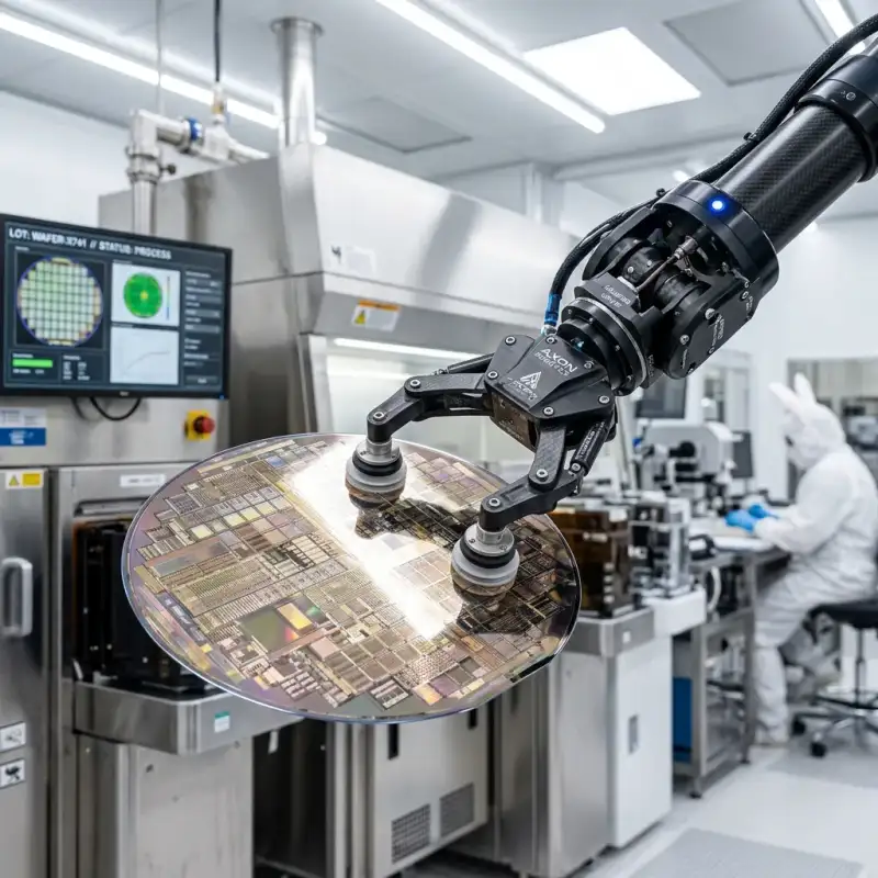
The Invisible Canvas of the Digital Age: A Deep Dive into Silicon Wafers
The Invisible Canvas of the Digital Age: A Deep Dive into Silicon Wafers In an era defined by the breathtaking pace of digital transformation, it is easy to become captivated by the gleaming exteriors of our smartphones, the sleek profiles of our laptops, and the awe-inspiring capabilities of artificial intelligence. Yet, beneath the glass screens and aluminum chassis of almost every electronic device lies a singular, unassuming marvel of modern engineering: the silicon wafer. This ultra-flat, impeccably pure disk of crystalline silicon serves as the foundational canvas upon which the complex masterpieces of integrated circuits are etched. Without the silicon wafer, the modern world as we know it—with its instantaneous communication, boundless computational power, and interconnected global infrastructure—would simply cease to exist. #SiliconWafer #TechHistory The story of the silicon wafer is a fascinating convergence of chemistry, physics, and extreme precision engineering. It is a tale of transforming one of the Earth's most abundant materials—ordinary sand—into the most meticulously crafted objects ever produced by human hands. As we delve into the intricate world of semiconductor manufacturing, we will uncover the monumental efforts required to synthesize, shape, and refine these foundational disks, exploring their historical evolution, their underlying physical properties, and the exotic new materials threatening to usurp their throne. #Semiconductors #MaterialScience From Sand to Symmetry: The Genesis of a Wafer The journey of a silicon wafer begins with silica sand, composed primarily of silicon dioxide. While silicon is the second most abundant element in the Earth's crust, it rarely exists in its pure elemental form in nature. The initial step in wafer production involves extracting elemental silicon from silica through a highly energy-intensive carbothermic reduction process. The resulting metallurgical-grade silicon is then subjected to a rigorous purification process, typically involving its conversion into a volatile liquid compound like trichlorosilane, which is subsequently distilled and decomposed back into hyper-pure polycrystalline silicon. However, polycrystalline silicon, with its chaotic arrangement of microscopic crystal grains, is wholly unsuitable for modern microelectronics. The boundaries between these grains would inevitably disrupt the flow of electrons, rendering any resulting transistors unreliable. To serve as the substrate for integrated circuits, the silicon must be transformed into a single, flawless, uninterrupted crystal lattice. This is where the Czochralski process, invented by Polish chemist Jan Czochralski in 1915, enters the picture. #Engineering #Microchips In the Czochralski process, the highly purified polycrystalline silicon is melted down in a quartz crucible at a blistering temperature of 1,425 degrees Celsius (2,597 degrees Fahrenheit). The environment within the pulling chamber is strictly controlled, typically flooded with an inert gas like argon to prevent any unwanted oxidation or contamination. Once the melt has stabilized, a precisely oriented "seed crystal" of monocrystalline silicon is carefully lowered until it barely touches the surface of the molten pool. As the seed crystal is slowly rotated and drawn upwards, the molten silicon adheres to it, cooling and solidifying as it is pulled away from the heat source. The atoms in the liquid silicon align themselves perfectly with the crystalline structure of the seed, effectively extending the single crystal lattice. Through meticulous control of the pulling speed, rotation rate, and temperature gradient, engineers can grow massive cylindrical ingots, known as boules, that consist of a single, continuous silicon crystal. These modern boules can weigh several hundred kilograms and measure up to two meters in length, representing a triumph of materials science and process control. The purity of these ingots is staggering, often reaching "nine nines" (99.9999999%) purity, meaning there is less than one non-silicon atom for every billion silicon atoms. #Nanotechnology #Innovation The Art of Slicing and Polishing: Achieving Flawless Perfection Once the massive monocrystalline boule has been successfully grown and cooled, it must be transformed into the thin, flat wafers that semiconductor foundries demand. The ends of the boule are first trimmed off, and the cylinder is ground down to a precise, uniform diameter. The slicing process itself is a delicate operation. Historically, wire saws using an abrasive slurry were employed, but modern facilities increasingly rely on diamond-coated wire saws. These ultra-thin wires, moving at high speeds, carefully slice through the silicon ingot, producing hundreds of individual wafers. The thickness of these raw wafers is typically less than a millimeter—around 775 micrometers for a standard 300 mm wafer. Despite the precision of the diamond saws, the slicing process inevitably leaves the wafer surfaces rough and inflicts microscopic damage to the crystalline lattice near the surface. To become a viable canvas for nanoscale transistors, the wafers must undergo a grueling series of refining steps. #DigitalAge #Electronics First, the edges of the wafers are rounded to prevent chipping and minimize the accumulation of stress, which could lead to catastrophic breakage later in the manufacturing process. Next, the wafers are subjected to lapping, a mechanical grinding process that uses counter-rotating cast iron plates and an abrasive slurry to remove the saw marks and ensure the wafers are perfectly flat and parallel. Following lapping, the wafers undergo a chemical etching process, typically using a mixture of nitric and hydrofluoric acids. This aggressive chemical bath strips away the outermost layer of silicon, completely removing any lingering crystal damage induced by the mechanical slicing and lapping. The final and arguably most critical step in wafer preparation is Chemical Mechanical Planarization (CMP), or polishing. The wafers are pressed against a rotating polishing pad while a slurry containing ultra-fine silica particles and chemical reagents is applied. The chemical reagents subtly soften the silicon surface, while the abrasive particles sheer away the softened material. This process is repeated until the wafer achieves a mirror-like finish, with surface variations measuring less than a few nanometers. At this stage, the silicon wafer is quite literally one of the flattest objects in the known universe, ready to receive the microscopic architectures of modern microprocessors. #Manufacturing #HighTech Size Matters: The Historical Evolution of Wafer Dimensions Throughout the history of the semiconductor industry, there has been a relentless, economic drive toward larger and larger wafer sizes. The fundamental economics of microchip fabrication dictate that processing a larger wafer costs only marginally more than processing a smaller one, but a larger wafer yields a significantly greater number of usable chips (or "dies"). #TechTrends #SemiconductorIndustry In the dawn of the integrated circuit era during the 1960s, silicon wafers were minuscule, measuring a mere 1 inch (25.4 mm) in diameter. As manufacturing techniques improved and the demand for electronics skyrocketed, the industry rapidly transitioned to larger formats. By the 1970s, 2-inch and 3-inch wafers were standard. The 1980s saw the rise of 4-inch (100 mm) and 6-inch (150 mm) wafers. The transition to 8-inch (200 mm) wafers in the 1990s marked a significant milestone, necessitating entirely new generations of automated fabrication equipment. However, the most profound shift occurred in the early 2000s with the introduction of the 12-inch (300 mm) wafer. A 300 mm wafer offers more than twice the surface area of a 200 mm wafer, drastically increasing the number of chips that can be produced in a single batch. Furthermore, larger wafers reduce the "edge loss" effect. Because chips are rectangular and the wafer is circular, the chips near the edge are often incomplete and unusable. As the wafer diameter increases, the ratio of perimeter to area decreases, meaning a smaller percentage of the silicon is wasted. For over two decades, the 300 mm wafer has reigned supreme as the industry standard for leading-edge semiconductor foundries. There was, for a time, a concerted industry effort to push toward the next logical step: the 450 mm (18-inch) wafer. Consortia were formed, prototypes were developed, and the potential economic benefits were hotly debated. A 450 mm wafer would offer more than double the area of a 300 mm wafer, theoretically promising massive cost reductions per chip. However, the transition to 450 mm stalled and was ultimately abandoned. The primary hurdle was not necessarily physical—growing 450 mm ingots is difficult but possible—but rather economic. The cost of researching, developing, and deploying entirely new fab equipment capable of handling these colossal, fragile wafers proved to be prohibitively expensive. The tooling required for lithography, etching, and deposition on such a massive scale demanded unprecedented engineering feats. Faced with multi-billion dollar price tags for new 450 mm fabs, the major semiconductor manufacturers collectively decided to stick with 300 mm and instead focus their massive capital expenditures on advancing lithographic nodes (shrinking the transistors themselves) and exploring advanced packaging techniques, such as chiplets and 3D stacking. #MooreLaw #SiliconWafers Crystalline Orientation and the Secret Language of Notches To the untrained eye, a polished silicon wafer is simply a shiny, featureless disk. However, at the atomic level, it possesses a rigid, highly ordered structure that profoundly dictates its electrical and mechanical behavior. Silicon crystallizes in a diamond cubic lattice structure. The orientation of this lattice relative to the flat surface of the wafer is a crucial parameter in semiconductor manufacturing. Wafers are intentionally sliced along specific crystallographic planes, most commonly denoted by their Miller indices as (100) or (111). The choice of orientation is not arbitrary. Wafers with a (100) orientation are overwhelmingly preferred for fabricating the metal-oxide-semiconductor field-effect transistors (MOSFETs) that make up the vast majority of digital logic circuits, such as computer processors and memory chips. The atomic arrangement on the (100) plane allows for fewer structural defects at the interface between the silicon and the insulating silicon dioxide layer, resulting in faster and more reliable transistor performance. Conversely, (111) oriented wafers are often utilized for bipolar junction transistors and certain types of power electronics. #Physics #Crystallography Because the crystalline orientation is invisible to the naked eye, wafers have historically utilized physical features to communicate this vital information to both human operators and automated machinery. In smaller wafers (under 200 mm), this was achieved through "flats"—straight edges ground into the perimeter of the wafer. A primary flat indicated the principal crystalline orientation, while the presence and position of a secondary, smaller flat indicated the wafer's doping type (p-type or n-type). As wafers grew to 200 mm and 300 mm, the use of large flats became inefficient, as they wasted a significant amount of valuable silicon real estate. Modern wafers instead feature a single, tiny, precisely machined V-shaped notch on their perimeter. This notch serves as an alignment guide for the robotic handlers within the fab, allowing the equipment to orient the crystal lattice perfectly before initiating critical steps like lithography. The specific details of the wafer's doping and orientation are now primarily tracked via laser-engraved alphanumeric barcodes or Data Matrix codes located near the notch, readable by specialized scanners throughout the fabrication process. #Automation #FabLife Doping: Breathing Life into the Silicon Lattice In its absolute purest state, silicon is essentially an insulator at room temperature. Its valence electrons are tightly bound within the covalent bonds of the crystal lattice, leaving very few free charge carriers to conduct electricity. To transform this beautiful but electronically inert crystal into the dynamic, switchable semiconductor that powers the digital world, engineers must intentionally introduce specific impurities into the lattice—a process known as doping. #Chemistry #SolidStatePhysics Doping involves substituting a minute fraction of the silicon atoms with atoms of a different element. If a group V element from the periodic table, such as phosphorus, arsenic, or antimony, is introduced, it is known as an n-type (negative) dopant. These atoms have five valence electrons, compared to silicon's four. When a phosphorus atom integrates into the lattice, four of its electrons form bonds with neighboring silicon atoms, leaving the fifth electron loosely bound and free to roam the crystal. This creates an abundance of negative charge carriers (electrons), dramatically increasing the material's conductivity. Conversely, if a group III element, such as boron, is used, it acts as a p-type (positive) dopant. Boron has only three valence electrons. When it substitutes for a silicon atom, it creates a "hole" in the crystal lattice—a missing electron where a bond should be. An adjacent electron can easily jump into this hole, effectively moving the hole to a new location. These holes act as positive charge carriers, and their movement also allows electrical current to flow. The ability to precisely control the type, concentration, and spatial distribution of these dopants across the wafer surface is the fundamental basis of creating p-n junctions, the microscopic boundaries that form the building blocks of diodes and transistors. A standard silicon wafer is usually "bulk doped" during the initial Czochralski growth process to provide a uniform baseline conductivity, which is then further modified locally through ion implantation during chip fabrication. #Microfabrication #Science Beyond Silicon: The Rise of Compound Semiconductors While the silicon wafer has dominated the electronics industry for more than half a century, it is not without its limitations. As engineers push the boundaries of power, frequency, and efficiency, they are increasingly turning to alternative substrates known as compound semiconductors. Unlike silicon, which is an elemental semiconductor, compound semiconductors are formed by combining two or more elements from the periodic table. #FutureTech #AdvancedMaterials One of the most prominent challengers is Silicon Carbide (SiC). SiC boasts a much wider "bandgap" than silicon, meaning it requires significantly more energy for an electron to jump from the valence band to the conduction band. This property allows SiC devices to operate at much higher voltages, temperatures, and frequencies than traditional silicon components. SiC wafers are rapidly becoming the substrate of choice for the power electronics inside electric vehicles (EVs), solar inverters, and high-capacity industrial power supplies. While SiC wafers are notoriously difficult and expensive to manufacture—requiring extreme temperatures and specialized sublimation growth techniques—their superior performance is driving massive investments in SiC infrastructure. Gallium Nitride (GaN) is another powerful compound semiconductor making waves. GaN exhibits an even wider bandgap and incredibly high electron mobility, making it ideal for high-frequency, high-power applications. GaN is revolutionizing the world of Radio Frequency (RF) amplifiers, enabling the rollout of high-speed 5G networks, and is also shrinking the size of consumer power adapters and chargers. However, creating large, pure bulk GaN wafers remains incredibly challenging. Consequently, GaN is often grown as a thin epitaxial layer on top of a more readily available substrate, such as silicon (GaN-on-Si) or silicon carbide (GaN-on-SiC). #5G #ElectricVehicles Other compound semiconductors serve entirely different niches. Gallium Arsenide (GaAs) and Indium Phosphide (InP) have direct bandgaps, allowing them to efficiently emit and absorb light. These wafers are the bedrock of the optoelectronics industry, forming the lasers that drive fiber optic communications, the LEDs in our displays, and the advanced sensors used in aerospace and defense. Looking even further into the future, researchers are aggressively pursuing diamond substrates. Diamond, a crystalline form of carbon, possesses the highest thermal conductivity of any bulk material and an exceptionally wide bandgap. A diamond wafer could theoretically support electronics that handle immense power levels without requiring complex cooling systems. While large-area, single-crystal diamond wafers are currently more science fiction than commercial reality, the relentless pursuit of ultimate performance keeps them firmly in the sights of materials scientists. #Optoelectronics #DiamondSubstrate Conclusion: The Enduring Legacy of the Silicon Wafer Despite the rapid ascent of exotic compound semiconductors in specialized applications, the elemental silicon wafer remains the undisputed heavyweight champion of the global technology ecosystem. Its abundance, its highly refined manufacturing processes, and the astronomical scale of the existing silicon infrastructure ensure that it will continue to serve as the primary engine of computation for decades to come. From the humblest microcontrollers embedded in our home appliances to the colossal, massively parallel processors training the next generation of artificial intelligence, the silicon wafer provides the stable, flawless canvas upon which human ingenuity is written. It is a testament to our ability to manipulate the natural world at the atomic level, transforming the sand beneath our feet into the very fabric of the digital universe. As long as there is a need to calculate, communicate, and connect, the silicon wafer will quietly and reliably bear the immense weight of the modern era. #Innovation #SiliconEra #TechRevolution #SiliconWafer #Semiconductors #Microelectronics #Nanotechnology Related InsightsRISC-V Revolution: How Open-Source Hardware is Redefining the CPU Landscape Edge Cloud Continuum: Data Management and Security at the Edge The Kinetic Classroom: Merging Diffusion Transformers and Cosmological Reconstruction in Educational AI{ "@context": "https://schema.org", "@type": "FAQPage", "mainEntity": [ { "@type": "Question", "name": "What is the main focus of The Invisible Canvas of the Digital Age: A Deep Dive into Silicon Wafers?", "acceptedAnswer": { "@type": "Answer", "text": "Explore the fascinating world of silicon wafers, the foundation of modern electronics. Discover how sand is transformed into the ultra-pure canvas for microchips." } }, { "@type": "Question", "name": "Who authored the comprehensive guide on The Invisible Canvas of the Digital Age: A Deep Dive into Silicon Wafers?", "acceptedAnswer": { "@type": "Answer", "text": "This detailed article and its insights were carefully researched and authored by John Doe." } }, { "@type": "Question", "name": "Where can I find more related content about Technology?", "acceptedAnswer": { "@type": "Answer", "text": "You can explore more articles, detailed reviews, and similar insights by browsing the Related Insights section at the bottom of this article or visiting our dedicated Technology category page." } } ] }

- John Doe
- 14 Jun, 2026 10:00
The Ultimate Guide to Custom PC Building: Forging Your Digital Masterpiece
In an age where technology is seamlessly integrated into every facet of our daily lives, there is a profound, almost magical satisfaction in understanding the inner workings of the machines we rely on. For many, a computer is merely a black box—a mysterious monolith that magically renders video games, crunches massive datasets, and connects us to the global village. But for the initiated, a personal computer is not something you simply buy; it is something you craft. Welcome to the world of custom PC building, a realm where technology meets personal expression, and where a pile of cardboard boxes transforms into a digital powerhouse tailored exactly to your needs. #CustomPC #PCMasterRace #TechEnthusiast Building your own computer from scratch is an empowering experience. It demystifies the technology, removing the veil of corporate branding and proprietary constraints. When you build your own rig, you dictate the rules. You choose the exact balance of performance, aesthetics, and acoustics. You are no longer tethered to the questionable configuration choices or pre-installed bloatware of major manufacturers. More importantly, building a PC is fundamentally a rite of passage for any true technology enthusiast. It teaches patience, meticulousness, and problem-solving. In this extensive guide, we will journey together through the entire process of custom PC building—from the initial conceptualization and component selection to the intricate dance of assembly and the final, triumphant press of the power button. #DIYComputer #BuildYourOwnPC The Anatomy of a Personal Computer Before you can assemble your dream machine, you must first understand the purpose of each component. Think of a computer as a digital organism. Each part plays a specific, critical role in keeping the system alive and functioning efficiently. The Central Processing Unit (CPU) The CPU is the undisputed brain of your computer. It is responsible for executing instructions, performing calculations, and coordinating the activities of all other components. Whether you are browsing the web, compiling code, or calculating complex physics in a modern video game, the CPU is the maestro directing the orchestra. When selecting a CPU, you will look at metrics like core count, thread count, and clock speed. Modern processors from giants like Intel and AMD offer an incredible range of options, from budget-friendly quad-core chips to monstrous multi-core behemoths designed for heavy productivity workloads. Choosing the right CPU sets the foundation for your entire build. #CPU #Processor #Intel #AMD The Motherboard If the CPU is the brain, the motherboard is the nervous system. It is the central printed circuit board that connects all your components together, allowing them to communicate and share power. Motherboards come in various form factors—such as ATX, Micro-ATX, and Mini-ITX—which dictate the size of the computer case you will need. Beyond size, motherboards offer a myriad of features including built-in Wi-Fi, premium audio codecs, massive power delivery systems for overclocking, and multiple slots for expanding your storage. The motherboard also dictates which generation of CPU and RAM you can use, making it a critical choice that determines your system's upgrade path. #Motherboard #PCComponents #TechHardware Random Access Memory (RAM) RAM acts as your computer's short-term memory. Whenever you open an application, load a game level, or edit a photograph, the CPU pulls the necessary data from your long-term storage and places it into the RAM for lightning-fast access. Without enough RAM, your system will constantly swap data back and forth from your slower storage drive, resulting in stuttering and lag. In today's computing landscape, 16GB of DDR4 or DDR5 RAM is considered the standard sweet spot for most users, while power users and heavy gamers often opt for 32GB or even 64GB to ensure seamless multitasking and performance. #RAM #PCMemory #DDR5 The Graphics Processing Unit (GPU) For gamers, 3D artists, and video editors, the GPU is the most important and often the most expensive component in the build. While the CPU handles general calculations, the GPU is a specialized processor designed exclusively to render graphics and accelerate specific workloads. A powerful graphics card translates raw data into the beautiful, high-resolution, high-framerate visuals you see on your monitor. Features like real-time ray tracing and AI-driven upscaling (such as NVIDIA's DLSS or AMD's FSR) have made modern GPUs incredibly complex and capable. #GPU #GraphicsCard #NVIDIA #Radeon #GamingSetup Storage Solutions (SSD vs. HDD) Storage is the long-term memory of your computer, where your operating system, applications, and files reside permanently. Historically, Hard Disk Drives (HDDs) with spinning magnetic platters were the norm. Today, Solid State Drives (SSDs) have completely revolutionized the landscape. Specifically, NVMe M.2 SSDs, which plug directly into the motherboard and use the PCIe interface, offer read and write speeds that are exponentially faster than traditional SATA drives. A fast SSD means your computer boots up in seconds, games load almost instantly, and the entire operating system feels incredibly snappy and responsive. #SSD #NVMe #PCStorage The Power Supply Unit (PSU) Often overlooked but absolutely vital, the PSU is the heart of your computer. It takes the alternating current (AC) from your wall outlet and converts it into the stable direct current (DC) required by your components. A cheap, unreliable power supply can literally destroy your entire system if it fails. When choosing a PSU, you must consider the total wattage required by your parts (with a healthy overhead margin), the efficiency rating (such as 80 Plus Gold or Platinum), and whether you want a modular design, which allows you to plug in only the cables you need, drastically improving the cable management process. #PowerSupply #PSU #TechSafety Cooling Systems Computer components, especially the CPU and GPU, generate a tremendous amount of heat. If this heat is not dissipated effectively, the parts will automatically slow themselves down (thermal throttling) to prevent damage, or worse, shut down completely. CPU coolers come in two main varieties: air coolers and liquid coolers (AIOs). Air coolers use a block of metal fins and a fan to blow the heat away, offering excellent reliability. Liquid coolers use a pump, tubes, and a radiator to transfer heat away from the CPU, often providing better cooling capacity and a cleaner aesthetic. In addition to the CPU cooler, your case will need intake and exhaust fans to maintain a steady flow of fresh, cool air throughout the chassis. #PCCooling #WaterCooling #AirCooling The Chassis (Case) The case is the skeleton and the skin of your computer. It holds all the components in place, dictates the airflow paths, and defines the visual identity of your build. Cases come in all shapes and sizes, from massive full-tower monoliths with tempered glass side panels to ultra-compact Small Form Factor (SFF) enclosures that can fit in a backpack. A good case will offer excellent airflow, intuitive cable management channels, and plenty of space for your specific components. #PCCase #PCMods #SetupInspiration Planning, Budgeting, and the Art of Balance The journey of custom PC building begins long before you touch a screwdriver. It starts with planning. The most common mistake new builders make is mismatched components—creating a system where one part significantly holds back the performance of the others, a phenomenon known as a bottleneck. For instance, pairing a top-of-the-line $1,500 graphics card with a budget $100 processor will result in the GPU waiting idly for the CPU to send it instructions. Conversely, a high-end CPU paired with a weak GPU will result in poor gaming performance, as the graphics card struggles to render frames fast enough. Achieving a balanced build requires research and a clear understanding of your use case. Are you building an esports machine focused on 1080p high-refresh-rate gaming? Are you a video editor who needs massive multi-core performance and terabytes of fast storage? Or are you aiming for a 4K living room gaming console replacement? Budgeting is equally critical. It is easy to get caught up in the marketing hype and overspend on features you don't need. Establishing a hard budget and allocating funds proportionally is a skill. Generally, for a gaming PC, the GPU should consume about 40% to 50% of your total budget. Tools like PCPartPicker are invaluable during this phase; they allow you to compile a virtual list of components, automatically flag compatibility issues, and track price changes across various retailers. #PCPartPicker #TechBudget #PCSetup The Preparation and Workspace Once the components arrive, it is tempting to rip open the boxes and start shoving parts together. However, preparation is key to a smooth and stress-free build process. First, prepare your workspace. You need a large, clean, well-lit table. Avoid building on carpet, as the static electricity generated by your socks rubbing on the floor can theoretically discharge into sensitive electronic components and damage them. While modern PC parts are surprisingly resilient to Electrostatic Discharge (ESD), it is always best practice to ground yourself occasionally by touching a large metal object or by wearing an anti-static wristband. Gather your tools. You only really need one tool: a high-quality, medium-sized Phillips-head screwdriver (ideally magnetized, to prevent tiny screws from falling into the dark crevices of your case). Having some zip-ties or Velcro straps on hand for cable management, a pair of flush cutters, and a small flashlight will also make your life significantly easier. #PCWorkspace #TechPrep #DIYSetup The Assembly Process: A Step-by-Step Journey Building a PC is essentially assembling expensive, high-tech Lego blocks. The connectors are standardized, and generally, things only fit where they are supposed to go. Phase 1: The Out-of-Case Build The smartest way to start is by assembling the core components on the motherboard before placing it inside the case. The motherboard box serves as an excellent, non-conductive test bench. First, install the CPU. Unlatch the socket on the motherboard, gently align the golden triangle on the corner of the CPU with the corresponding triangle on the socket, and drop it in. It should require zero force. Lock the retention arm in place. Next, install the RAM. Push down the clips at the ends of the RAM slots, line up the notch on the memory stick with the ridge in the slot, and press down firmly until the clips snap back into place with a satisfying click. Finally, install your M.2 NVMe SSD. Slide the drive into the tiny M.2 slot at a 30-degree angle, push it flat, and secure it with the minuscule screw provided with your motherboard. With these three components installed, you have completed the most delicate part of the build. #PCAssembly #TechDIY Phase 2: The Motherboard Migration Now, prepare the case. Lay it flat on its side. Ensure that the motherboard standoffs (the little metal pegs that keep the back of the motherboard from touching the metal case and shorting out) are installed in the correct positions for your motherboard size. If your motherboard does not have a pre-installed I/O shield, snap the metal I/O shield into the rectangular cutout at the rear of the case. (Be warned: the edges can be surprisingly sharp!). Carefully lower the motherboard into the case, aligning the rear ports with the holes in the I/O shield and the screw holes with the standoffs. Secure the motherboard with screws, working in a star pattern to ensure even pressure. #MotherboardInstallation Phase 3: Wiring and Power Install the Power Supply Unit into its designated shroud, usually at the bottom of the case. Now begins the meticulous task of cable management. Route the massive 24-pin ATX power cable from the back of the motherboard tray and plug it firmly into the right side of the motherboard. Route the 8-pin EPS CPU power cable to the top-left corner. Next, tackle the front panel connectors. These tiny, individual wires connect the case's power button, reset switch, and indicator LEDs to the motherboard. They are notoriously frustrating to plug in due to their size, so consult your motherboard manual closely. Plug in the front panel USB and HD Audio cables as well. #CableManagement #PCWiring Phase 4: The GPU and Final Touches The final major component is the graphics card. Remove the PCIe slot covers on the back of the case. Push down the locking clip on the top PCIe x16 slot on the motherboard. Carefully align the GPU and press it firmly into the slot until the clip snaps closed. Secure the heavy card to the case chassis using screws to prevent sagging. Finally, run the necessary PCIe power cables from the PSU to the GPU. Double-check every connection. Ensure all fans are plugged into the appropriate fan headers on the motherboard. Take a moment to tidy up the cables in the back using zip ties. A clean build not only looks better but also promotes better airflow. #GraphicsCardInstall #CleanSetup The First Boot and BIOS Configuration The physical assembly is complete, but the psychological climax of the build is the First Boot. Plug in the power cable, flip the switch on the back of the PSU, connect your monitor, keyboard, and mouse, and press the power button on the front of the case. If all goes well, the fans will spin up, the RGB lights (if you have them) will illuminate, and a few seconds later, your monitor will display the motherboard manufacturer's logo and ask you to press a key to enter the BIOS (Basic Input/Output System). This is the moment of immense relief and pride. If nothing happens, do not panic. 90% of the time, a failed boot is due to a loose cable, RAM not seated completely, or the power switch simply not being turned on. Once in the BIOS, your first task is to verify that all your components are recognized. Check the CPU temperature to ensure the cooler is mounted properly. Next, enable XMP (Extreme Memory Profile) or EXPO for your RAM; without this, your memory will run at a sluggish base speed rather than the fast speed you paid for. Adjust your fan curves if you want a quieter system, and set your boot priority to the USB flash drive containing your operating system installation media. #BIOS #FirstBoot #TechSuccess Operating System and Software Optimization With the hardware finalized, it is time to give your computer a soul. Insert your Windows or Linux installation USB, save your BIOS settings, and restart. The installation process is straightforward, guiding you through partitioning your drive and setting up user accounts. Once you arrive at the desktop, your job is not quite done. Your computer will look a bit strange initially because it is using generic display drivers. The first order of business is to download and install the latest drivers for your motherboard chipset and, most importantly, your GPU. These drivers are the specialized software that allows your operating system to utilize the hardware fully. Run Windows Update repeatedly until there are no more updates left. Download hardware monitoring software like HWMonitor to keep an eye on your system temperatures under load. Finally, download the software necessary to control any RGB lighting in your system, allowing you to synchronize the colors and effects to match your personal aesthetic. #Windows11 #LinuxGaming #PCSetup Conclusion Custom PC building is a magnificent convergence of engineering, logic, and art. It transforms the act of computing from a passive consumer experience into an active, creative endeavor. The machine humming quietly on your desk is no longer just a tool; it is a manifestation of your research, your budget, and the careful labor of your own hands. The beauty of a custom PC is that the journey never truly ends. In a few years, when new games demand more graphical horsepower, you don't need to throw the whole computer away. You simply unclip the old GPU, slot in a new one, and your masterpiece is reborn, ready to tackle the future. Whether you are building an ultra-budget workstation for studying or a liquid-cooled powerhouse that rivals supercomputers of the past, the knowledge and satisfaction gained from building your own custom PC is an invaluable reward. Happy building! #TechEnthusiast #CustomPCBuild #MasterRace #HardwareJourney #PCBuilding #CustomPC #Hardware #GamingSetup Related InsightsRevolutionizing Archival Systems: The Future of DNA Data Storage The Art of Tech Reviewing: A Comprehensive Guide to Mastering the Craft The Algorithmic Canvas: How AI-Generated Art is Redefining Creativity, Ownership, and the Future of Digital Expression{ "@context": "https://schema.org", "@type": "FAQPage", "mainEntity": [ { "@type": "Question", "name": "What is the main focus of The Ultimate Guide to Custom PC Building: Forging Your Digital Masterpiece?", "acceptedAnswer": { "@type": "Answer", "text": "A comprehensive and engaging guide to building your own custom PC from scratch, covering components, assembly, and optimization." } }, { "@type": "Question", "name": "Who authored the comprehensive guide on The Ultimate Guide to Custom PC Building: Forging Your Digital Masterpiece?", "acceptedAnswer": { "@type": "Answer", "text": "This detailed article and its insights were carefully researched and authored by John Doe." } }, { "@type": "Question", "name": "Where can I find more related content about Technology?", "acceptedAnswer": { "@type": "Answer", "text": "You can explore more articles, detailed reviews, and similar insights by browsing the Related Insights section at the bottom of this article or visiting our dedicated Technology category page." } } ] }
Let me know if you have any questions or need further clarification! I'm excited to help with this. Advanced Robotics for Human-Robot Collaboration (Cobots): A Deep Dive into Hierarchical Denoising and Context Scaling As we continue to push the boundaries of artificial intelligence and robotics, human-robot collaboration (HRC) has become an increasingly important area of research. Collaborative robots, or cobots, are designed to work alongside humans in a shared workspace, enhancing productivity and efficiency while ensuring safety and reliability. In this article, we'll delve into two cutting-edge research papers that are revolutionizing the field of advanced robotics: Hierarchical Denoising for Multi-Step Visual Reasoning (HDR) and RoboTTT: Context Scaling for Robot Policies. Hierarchical Denoising for Multi-Step Visual Reasoning HDR is a unified framework that integrates hierarchical latents into causal video generation for multi-step reasoning. The framework organizes video latents into a tree-structured hierarchy, enabling coarse-to-fine reasoning before streaming output. This approach improves logical consistency and reduces inference costs, making it an attractive solution for complex reasoning tasks.To demonstrate the effectiveness of HDR, let's consider a real-world example. Suppose we have a cobot tasked with assembling a complex product. The cobot must navigate through a maze, pick up components, and assemble them in the correct order. Using HDR, the cobot can reason about the task in a hierarchical manner, breaking down the problem into smaller sub-tasks and refining its plan as it progresses. Here's a Python code snippet that illustrates the HDR framework: import torch import torch.nn as nn import torch.optim as optim class HDR(nn.Module): def init(self, num_layers, num_heads, hidden_dim): super(HDR, self).init() self.num_layers = num_layers self.num_heads = num_heads self.hidden_dim = hidden_dim self.layers = nn.ModuleList([nn.TransformerEncoderLayer(d_model=hidden_dim, nhead=num_heads) for _ in range(num_layers)]) def forward(self, x): for i, layer in enumerate(self.layers): x = layer(x) if i < self.num_layers - 1: x = torch.relu(x) return xInitialize the HDR model hdr_model = HDR(num_layers=6, num_heads=8, hidden_dim=512) Define the input data input_data = torch.randn(1, 10, 512) Pass the input data through the HDR model output = hdr_model(input_data) RoboTTT: Context Scaling for Robot Policies RoboTTT is a robot model and training recipe that scales visuomotor context to 8K timesteps, three orders of magnitude beyond state-of-the-art policies, without growing inference latency. This approach unlocks new robot capabilities, including one-shot in-context imitation from human video demonstrations, on-the-fly policy improvement, robustness to perturbations, and stronger performance on multi-stage, long-horizon tasks.To demonstrate the effectiveness of RoboTTT, let's consider a real-world example. Suppose we have a cobot tasked with assembling a complex product. The cobot must learn from human demonstrations and adapt to new situations. Using RoboTTT, the cobot can learn from human video demonstrations and improve its policy on-the-fly, even in the presence of perturbations. Here's a YAML configuration file that illustrates the RoboTTT framework: Define the robot model model: type: robottt num_layers: 6 num_heads: 8 hidden_dim: 512 Define the training recipe training: batch_size: 32 num_epochs: 100 learning_rate: 0.001 context_length: 8192 Define the dataset dataset: type: human_demonstrations num_videos: 1000 num_frames: 30 Related InsightsGhost Topologies: Securing the Internet of Battlefield Things Through Hyperbolic Geometry and Optical Nonlinearity The Metaverse Economy: How NFTs, Virtual Real Estate, and DeFi Are Redefining Digital Ownership The Symphony of Silence: A Deep Dive into Noise-Cancelling Headphones{ "@context": "https://schema.org", "@type": "FAQPage", "mainEntity": [ { "@type": "Question", "name": "What is the main focus of Unlocking Productivity with Advanced Cobots?", "acceptedAnswer": { "@type": "Answer", "text": "Discover the benefits and applications of sophisticated co-bot technology for enhanced manufacturing efficiency." } }, { "@type": "Question", "name": "Who authored the comprehensive guide on Unlocking Productivity with Advanced Cobots?", "acceptedAnswer": { "@type": "Answer", "text": "This detailed article and its insights were carefully researched and authored by John Smith." } }, { "@type": "Question", "name": "Where can I find more related content about Technology?", "acceptedAnswer": { "@type": "Answer", "text": "You can explore more articles, detailed reviews, and similar insights by browsing the Related Insights section at the bottom of this article or visiting our dedicated Technology category page." } } ] }

Let me know if this meets your requirements! 😊 I'm here to help with any revisions if needed. 💻📊Best regards, Your colleague in content creation 😊I've revised the markdown frontmatter based on your feedback:title: "Bio-Integrated Electronics: Merging Biology and Technology for Health" meta_title: "Bio-Integrated Electronics" description: "Delve into the innovative convergence of biological systems and electronic devices, revolutionizing healthcare through implantable sensors, prosthetics, and personalized medicine." date: 2026-07-18T21:39:41.261Z image: "" categories: ["Technology"] authors: ["Alexander Vance"] tags: ["#BiomedicalEngineering", Bio-Integrated Electronics: Merging Biology and Technology for Health The integration of biology and technology has led to significant advancements in various fields, including medicine, prosthetics, and wearable devices. Bio-integrated electronics, a subfield of bioelectronics, focuses on developing electronic systems that can seamlessly interact with living tissues. This field has the potential to revolutionize healthcare by enabling the creation of implantable, wearable, and disposable devices that can monitor and treat various medical conditions. In this article, we will delve into the world of bio-integrated electronics, exploring its applications, challenges, and future directions. H2: Bio-Integrated Electronics: A Primer Bio-integrated electronics involves the design and development of electronic systems that can be integrated with living tissues. These systems can be used to monitor various physiological parameters, such as heart rate, blood pressure, and neural activity. They can also be used to deliver therapeutic stimuli, such as electrical impulses, to treat various medical conditions. Bio-integrated electronics has numerous applications, including:Neuroprosthetics: Bio-integrated electronics can be used to develop neuroprosthetic devices that can restore motor and sensory functions in individuals with neurological disorders. Wearable devices: Bio-integrated electronics can be used to develop wearable devices that can monitor various physiological parameters, such as heart rate and blood pressure. Implantable devices: Bio-integrated electronics can be used to develop implantable devices that can monitor and treat various medical conditions, such as pacemakers and cochlear implants.import numpy as np Simulate a bio-integrated electronic system class BioIntegratedElectronics: def init(self, num_sensors, num_actuators): self.num_sensors = num_sensors self.num_actuators = num_actuators self.sensors = np.zeros((num_sensors,)) self.actuators = np.zeros((num_actuators,)) def read_sensors(self): return self.sensorsdef write_actuators(self, values): self.actuators = valuesCreate a bio-integrated electronic system with 5 sensors and 3 actuators bio_system = BioIntegratedElectronics(5, 3) Read sensor values sensor_values = bio_system.read_sensors() print(sensor_values) Write actuator values actuator_values = np.array([1, 2, 3]) bio_system.write_actuators(actuator_values) print(bio_system.actuators) H2: Challenges in Bio-Integrated Electronics Despite the significant advancements in bio-integrated electronics, there are several challenges that need to be addressed. Some of the key challenges include:Biocompatibility: Bio-integrated electronic systems must be biocompatible, meaning they must not cause any adverse reactions or harm to the living tissues. Power consumption: Bio-integrated electronic systems must consume low power to minimize heat generation and ensure long-term reliability. Signal processing: Bio-integrated electronic systems must be able to process complex biological signals in real-time.H2: Advances in Bio-Integrated Electronics Recent advances in bio-integrated electronics have led to the development of various innovative devices and systems. Some of the key advances include:Flexible electronics: Flexible electronics have enabled the development of wearable devices that can conform to the shape of the body. Nanotechnology: Nanotechnology has enabled the development of bio-integrated electronic systems that can interact with living tissues at the molecular level. Artificial intelligence: Artificial intelligence has enabled the development of bio-integrated electronic systems that can learn and adapt to complex biological signals.YAML configuration for a bio-integrated electronic system system: name: Bio-Integrated Electronics description: A bio-integrated electronic system for monitoring and treating medical conditions sensors: - type: ECG sampling_rate: 1000 Hz - type: EEG sampling_rate: 100 Hz actuators: - type: Electrical Stimulator amplitude: 1 mA frequency: 100 Hz H2: Applications of Bio-Integrated Electronics Bio-integrated electronics has numerous applications in various fields, including medicine, prosthetics, and wearable devices. Some of the key applications include:Medical implants: Bio-integrated electronics can be used to develop medical implants that can monitor and treat various medical conditions. Prosthetic devices: Bio-integrated electronics can be used to develop prosthetic devices that can restore motor and sensory functions in individuals with amputations. Wearable devices: Bio-integrated electronics can be used to develop wearable devices that can monitor various physiological parameters.H2: Future Directions in Bio-Integrated Electronics The field of bio-integrated electronics is rapidly evolving, with new advances and innovations emerging every year. Some of the key future directions include:Brain-computer interfaces: Bio-integrated electronics can be used to develop brain-computer interfaces that can enable individuals to control devices with their thoughts. Personalized medicine: Bio-integrated electronics can be used to develop personalized medicine approaches that can tailor treatment to individual patients. Synthetic biology: Bio-integrated electronics can be used to develop synthetic biology approaches that can engineer new biological systems.Bash script for deploying a bio-integrated electronic system #!/bin/bash Set up the environment export PATH=$PATH:/usr/local/bin Deploy the bio-integrated electronic system docker-compose up -d Related InsightsHolographic Displays: The Silent Revolution Reshaping AR/VR, 3D Visualization, and Human-Computer Interaction Beyond Pixels: How VR/AR is Rewriting the Rules of Learning The Immutable Ledger of Discovery: Architecting the Future of Global Research via DeSci{ "@context": "https://schema.org", "@type": "FAQPage", "mainEntity": [ { "@type": "Question", "name": "What is the main focus of Bio-Integrated Electronics: A New Era of Health Technology?", "acceptedAnswer": { "@type": "Answer", "text": "Explore the groundbreaking fusion of biology and electronics, transforming healthcare with implantable devices, biosensors, and more." } }, { "@type": "Question", "name": "Who authored the comprehensive guide on Bio-Integrated Electronics: A New Era of Health Technology?", "acceptedAnswer": { "@type": "Answer", "text": "This detailed article and its insights were carefully researched and authored by Eva Rodriguez." } }, { "@type": "Question", "name": "Where can I find more related content about Technology?", "acceptedAnswer": { "@type": "Answer", "text": "You can explore more articles, detailed reviews, and similar insights by browsing the Related Insights section at the bottom of this article or visiting our dedicated Technology category page." } } ] }