The Invisible Canvas of the Digital Age: A Deep Dive into Silicon Wafers
-
 Emily Page
 - 01 Sep, 2026 10:45
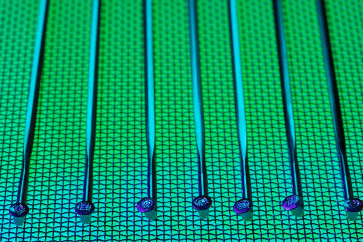
Beneath the polished glass of your smartphone and the rhythmic hum of the servers that power our global connectivity lies a substance so profoundly transformative that it has redefined the boundaries of human possibility. We treat technology as ephemeral, a cloud-based ether that exists everywhere and nowhere, yet its physical manifestation is anchored in something as tangible and ancient as the earth itself: sand. Specifically, the ultra-pure, crystalline silicon wafer. These discs, shimmering with a holographic iridescence, are the invisible canvases of the digital age, the fragile foundations upon which we have etched the entire library of human knowledge.
From Earth to Eternity: The Alchemy of Crystal Growth
The story of the silicon wafer begins not in a laboratory, but in the elemental furnace of the earth. Silicon is the second most abundant element in the crust, but to become a computer chip, it must undergo a rigorous purification process. The goal is to reach a level of purity known as “eleven nines”—99.999999999% pure. This is a level of refinement that borders on the spiritual; even a single errant atom of impurity can render the entire structure chaotic and unusable.
To create the wafer, high-purity polycrystalline silicon is melted in a crucible. This process, often referred to as the Czochralski method, involves dipping a tiny, perfectly oriented seed crystal into the molten pool. As the seed is slowly pulled upward and rotated, a single, flawless cylindrical ingot—a boules—is formed. It is a slow, meditative process. Imagine a single crystal structure, growing atom by atom, maintaining a perfect lattice orientation throughout its entire length. This ingot, often weighing hundreds of pounds, represents the raw potential of the digital world.

The Precision of the Blade
Once the ingot is cooled, it is sliced with wire saws impregnated with diamond dust. These blades move with surgical precision, carving the solid cylinder into discs often less than a millimeter thick. The surface must be polished until it reaches a mirror-like finish, free of any microscopic scratches or deformations.
This wafer is the canvas. It is a stage of absolute flatness, a pristine landscape where we will soon construct cities of light and electricity. When you hold a wafer in your hand, you are not merely looking at a piece of glass-like material; you are looking at a substrate that has been engineered to be the most perfect surface on the planet. If the topography of the Earth were scaled down to the smoothness of a silicon wafer, the Himalayas would be invisible to the naked eye.
Etching the Architecture of Thought
The actual process of turning a wafer into a functional brain for a computer—the integrated circuit—is perhaps the most sophisticated manufacturing feat in history. It is a process of photolithography, a form of high-tech printing that uses light to project patterns onto the wafer.
The wafer is coated with a light-sensitive chemical called a photoresist. Through a series of complex masks, ultraviolet light is shone onto the surface, creating intricate patterns of channels and gates. These patterns define the logic, the memory, and the processing power of the chip. Following exposure, the wafer is subjected to chemical etching or ion implantation, processes that carve away unwanted materials or inject specific impurities into the silicon to change its electrical properties.
We are, in essence, painting with light. We build layers upon layers, a vertical architecture of transistors that are so small that billions can fit on a single chip. It is a cathedral of microscopic proportions, where logic flows through gates that are only a few atoms wide.
The Invisible Library of Human Progress
Why do we not talk more about the wafer? Perhaps because it is designed to disappear. Once the chips are cut from the wafer, packaged into plastic or ceramic shells, and installed into devices, the wafer itself is gone, buried deep within the machinery. Yet, every book we read on a tablet, every photograph stored in the cloud, and every line of code that guides our autonomous vehicles began its life on that round, shimmering disc.
This technology has shifted the way we store history. In the past, we relied on paper and parchment, canvases made of pulp or animal skin. Now, our history is recorded in the displacement of electrons within a crystal lattice. We have moved from the ink of the quill to the light of the laser. The silicon wafer is the ultimate library, one that can hold the entire sum of human thought within a space no larger than a human fingernail.
Challenges at the Edge of Physics
As we push the boundaries of what is possible, we encounter the strange and unforgiving laws of quantum mechanics. When a transistor gate is only a few atoms thick, the electrons do not always behave as expected. They exhibit “tunneling,” where they skip over barriers as if they were ghosts.
This is the frontier of our current age. Engineers are now moving toward three-dimensional structures—FinFETs and Gate-All-Around (GAA) architectures—where the transistors are no longer flat, but standing upright like skyscrapers in a digital metropolis. The canvas is becoming a landscape of depth and complexity. We are not just building on the surface; we are building upward, seeking to pack more intelligence into every square millimeter of silicon.
The Future of the Crystalline Canvas
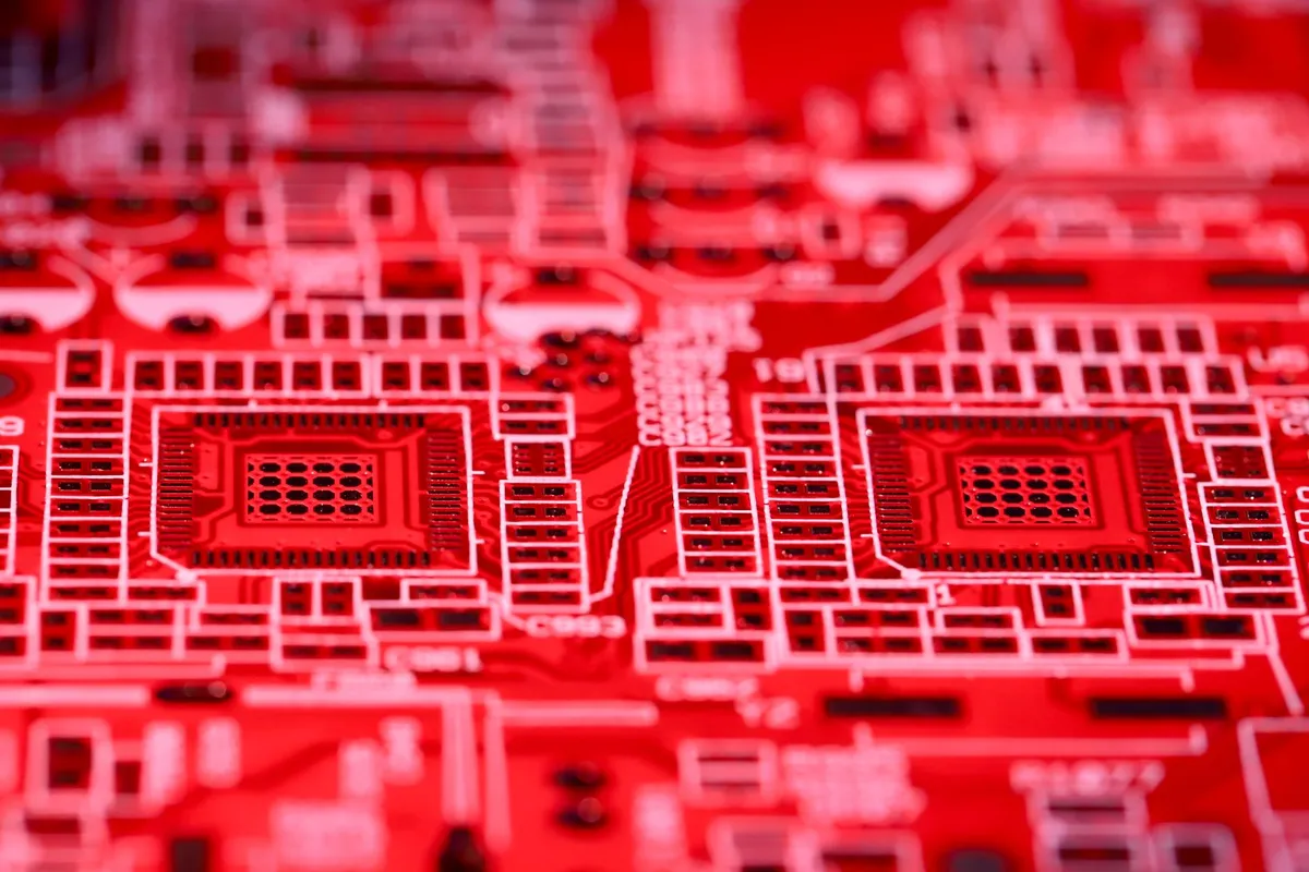
What lies beyond the current generation of wafers? Research into materials like gallium nitride and silicon carbide promises to handle higher voltages and heat, potentially transforming how we manage energy grid infrastructure and electric vehicles. We are even exploring the use of neuromorphic computing—chips designed to mimic the biological structure of the human brain.
The silicon wafer remains the constant. Despite the chatter about quantum computing and biological data storage, silicon’s role as the foundation of modern civilization is unlikely to be supplanted soon. It is a testament to the power of human ingenuity—that we took the most common material in the earth, and through relentless, exacting science, turned it into the very medium of modern consciousness.
When you look at your computer or smartphone again, remember the wafer. Remember the ingot grown from a single seed, the diamond-sawed slices, and the light-etched patterns that move at the speed of thought. You are looking at the culmination of a journey that began with the earth and ended with the stars, a canvas that holds not just data, but the story of us.
#SiliconWafers #SemiconductorHistory #ComputingArchitecture #MicrochipInnovation #DigitalFoundations